M4-R1 Introduction
Chapter 1 Product Overview
1.1 Scope of application
ShimetaPi M4-R1 V1.0 belongs to the ShimetaPi series motherboards. The RK3568B2 chip used is a low-power, high-performance processor. It is widely used in video terminal products, industrial automation terminals, and computing terminal products, such as: smart self-service terminals, O2O smart devices, industrial control hosts, robotic equipment, etc.
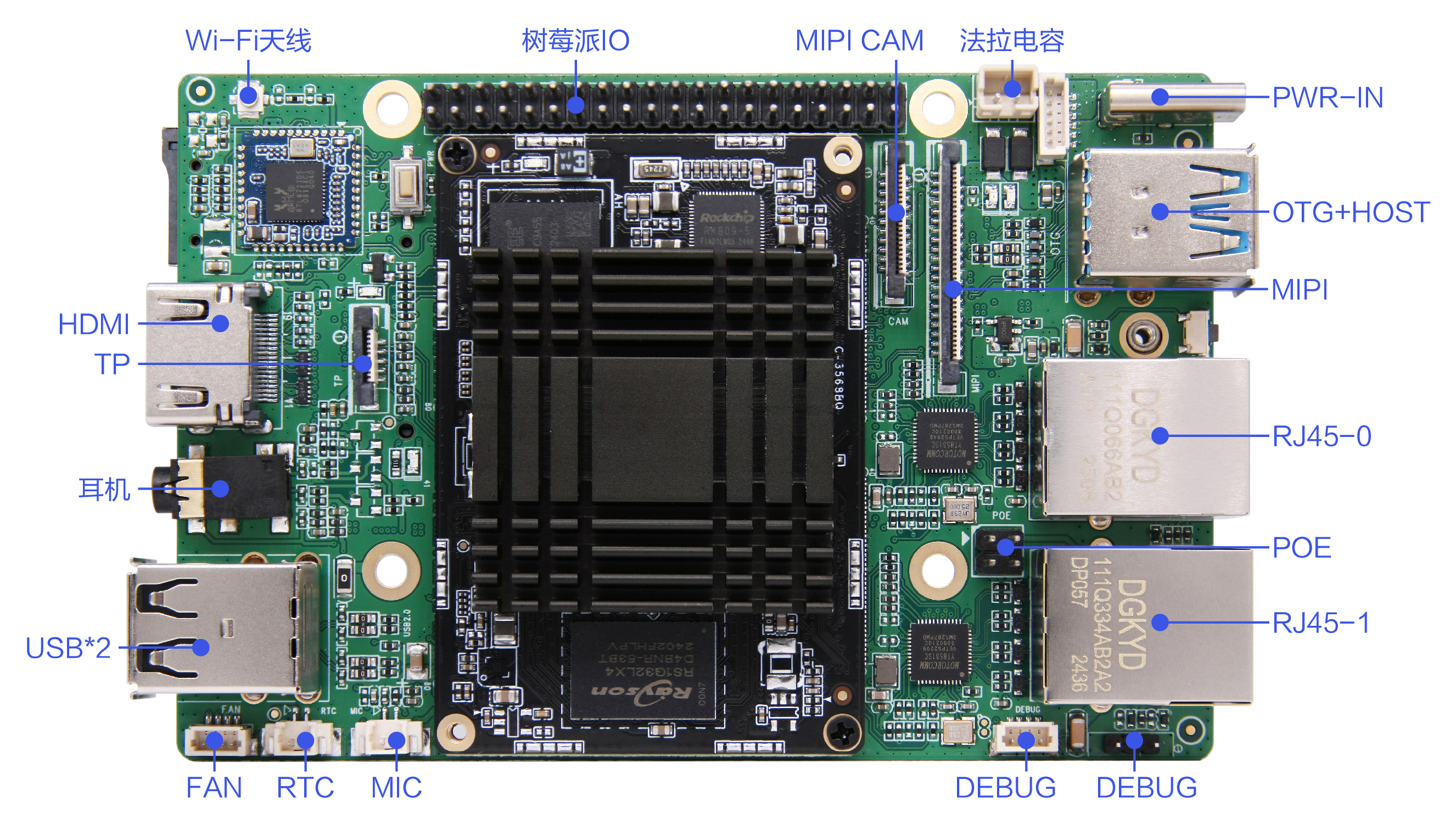
1.2 Appearance and interface diagram
front:
back:
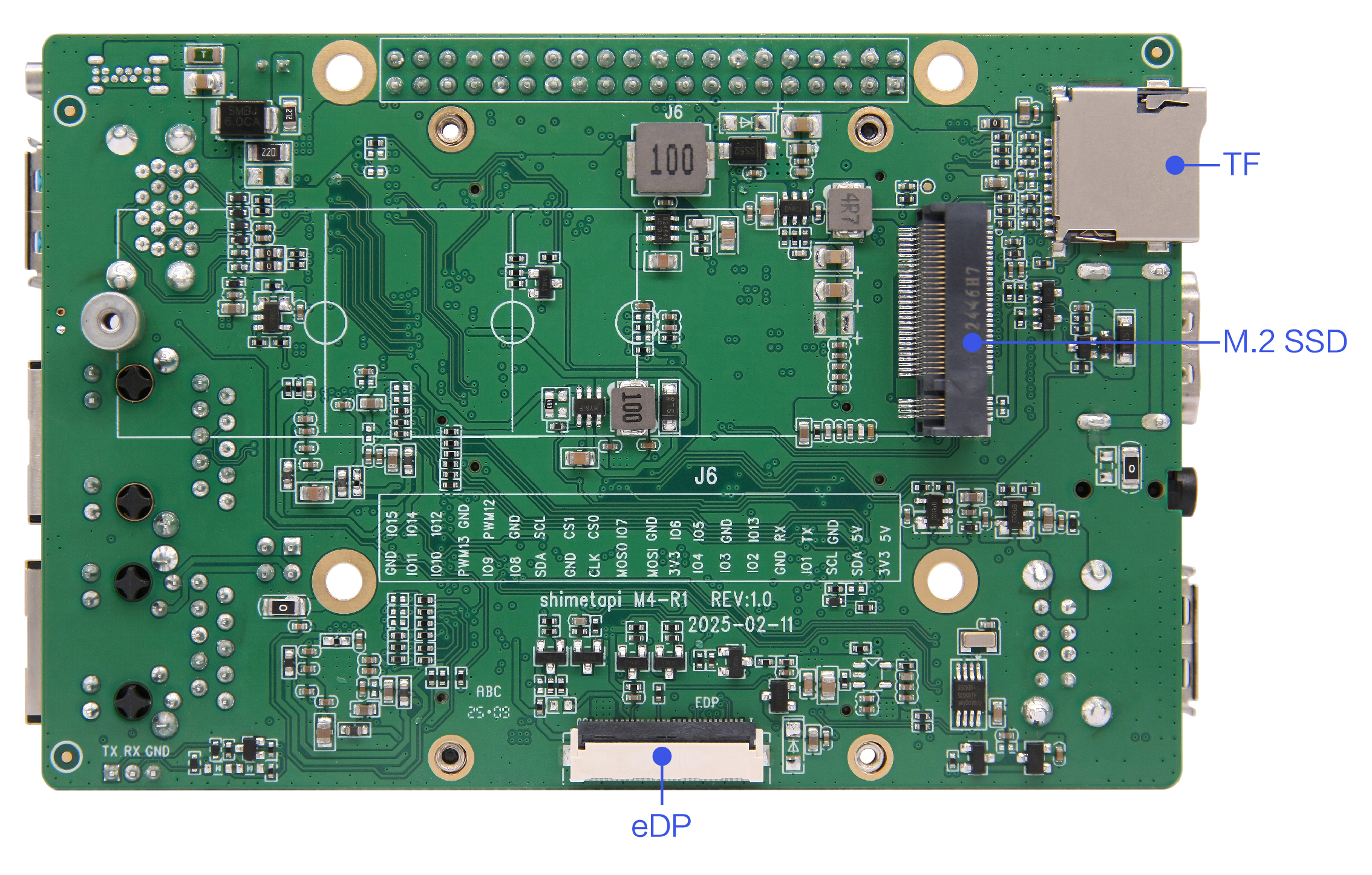
Front view:
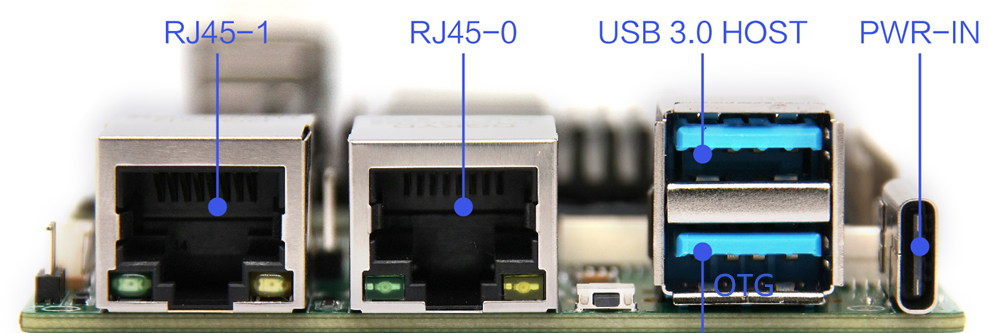
Photo Statement
The above photos were taken from a batch of boards produced by our company. Due to the continuous maintenance of the products, the boards actually shipped may not be consistent with the photos.
Chapter 2 Basic Function List
| Function | Describe |
|---|---|
| Board size | 110*73mm |
| CPU | Rockchip RK3568B2; quad-core 64-bit Cortex-A55; main frequency up to 2.0GHz |
| GPU | ARM G52 2EE; supports OpenGL ES 1.1/2.0/3.2, OpenCL 2.0, Vulkan 1.1; embedded high-performance 2D acceleration hardware |
| NPU | Support 1Tops computing power |
| operating system | Linux and open source Hongmeng system |
| Memory/Storage | Standard 4GB / Standard 32GB |
| HDMI output | 1-way, standard Type-A female connector, supports up to 4Kx2K@60Hz resolution |
| MIPI output | 1 channel, can directly drive MIPI interface LCD screens with various resolutions, and has supported 720*1280 resolution |
| MIPI Input | 1 channel, can support 800W pixels |
| edp output | 1 channel, can directly drive eDP interface LCD screens with various resolutions, and has supported 1920*1080 resolution |
| Headphone output | Support one-way three/four-band headphone insertion |
| USB interface | 1-way USB3.0 OTG, 1-way USB3.0 HOST, 2-way USB2.0 HOST |
| Serial Port | 1 TTL, 1 Debug |
| I2C Interface | 3 channels, can be connected to TP or peripherals with I2C interface |
| Raspberry Pi Interface | 1-way, 2*20PIN pin socket, spacing 2.0MM |
| Network support | Supports 2-way 10/100/1000M adaptive Ethernet; built-in Wi-Fi, supports Bluetooth 4.2 |
| storage | Support U disk, TF card expansion storage |
| RTC Real Time Clock | Support low power consumption |
| System Upgrade | Support local USB upgrade |
| key | 1 POWER ON button; 1 Uboot burning button |
| LED | 2-way, user programmable indicator lights |
Chapter 3 PCB Size and Interface Layout
3.1 PCB Dimensions
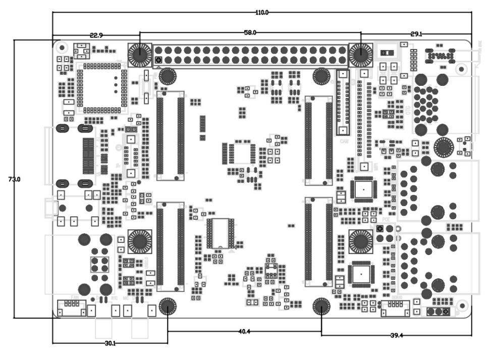
PCB : 8-layer board, thickness 1.6mm
PCBA: L _ W = 110mm_ 73mm
Screw hole specifications: ∮3.0mm x 4
Warning
Heat dissipation design
The actual size of the product shall prevail
3.2 Interface parameter description
Picture annotation instructions: The circle on the socket interface picture  indicates the first pin, and the red socket
  indicates the first pin
3.2.1 Power input (6pin/1.0mm)
(1) Functional description:
The board is powered by a 5V DC power supply, and is only allowed to be powered by the Type-C USB port and the 6pin1.0mm power socket.
When no external devices are connected and the load is empty, the 5V DC power supply must support a minimum current of 1000mA.
(2) Electrical definition:
| Serial number | definition | property | Describe | |
|---|---|---|---|---|
| 1 | 5V | enter | 5V Input | |
| 2 | 5V | enter | 5V Input | |
| 3 | 5V | enter | 5V Input | 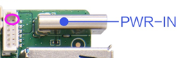 |
| 4 | GND | Ground | Ground | |
| 5 | GND | Ground | Ground | |
| 6 | GND | Ground | Ground | |
3.2.2 MIC interface (2pin/1.25mm)
(1) Functional description:
The motherboard has a MIC interface for connecting an external microphone.
(2) Electrical definition:
| Serial number | definition | property | Describe | |
|---|---|---|---|---|
| 1 | MIC+ | enter | MIC+ |  |
| 1 | MIC- | enter | MIC- | |
Warning
- Pay attention to the connection of the positive and negative poles of the MIC, and do not connect them in reverse;
- When there is no external load connected, the 5V DC power supply must support a minimum current of 1000mA.
3.2.3 RTC interface (2pin/1.25mm)
(1) Functional description:
The motherboard has a 2-pin 1.25mm pitch Wafer socket interface, which is used to power the system clock when the power is off.
(2) Electrical definition:
| Serial number | definition | property | describe | |
|---|---|---|---|---|
| 1 | RTC | enter | 3V input |  |
| 2 | GND | Ground | Ground | |
Warning
- When using the RTC battery, pay attention to whether the positive and negative poles are correct. Reverse connection may cause a short circuit, which may result in a risk of fire and explosion.
- If the RTC time is found to be inaccurate during use, please replace the RTC battery in time and choose the correct 3V, CR2036 button battery. If you need to use a battery with a wire, please contact FAE to provide the corresponding model specifications.
3.2.4 DEBUG serial port interface (4pin/1.0mm)
(1) Functional description:
Used for printing out system logs and UART Debug of RK3588.
(2) Electrical definition:
| Serial number | definition | property | describe | |
|---|---|---|---|---|
| 1 | GND | Ground | Ground |  |
| 2 | UART-RX | enter | RX2 | |
| 3 | UART-TX | Output | TX2 | |
| 4 | NC | --- | Alley-oop | |
Warning
- Pay attention to whether the TX and RX connections are correct.
- The default serial port printing baud rate is 1500000bps.
- If the level of the connected serial port is higher than 3.3V, an isolation circuit or level conversion circuit is required, otherwise the main control and equipment will be burned out.
3.2.5 FAN interface (4pin/1.0mm)
(1) Functional description:
The board has 1 fan interface, supports 5V fans, and supports PWM speed adjustment.
(2) Electrical definition:
| Serial number | definition | property | describe | |
|---|---|---|---|---|
| 1 | 5V | power supply | 5V power supply |  |
| 2 | PWM | Output | Fan speed adjustment control | |
| 3 | GND | Ground | Ground | |
| 4 | NC | --- | Alley-oop | |
Warning
- When installing the fan, pay attention to whether the pin definitions are consistent.
3.2.6 TP interface (10pin/0.5mm)
(1) Functional description:
The board supports TP screen connected to I2C interface, and the interface is in the form of 10pin 0.5mm pitch vertical FPC socket.
(2) Electrical definition:
| Serial number | definition | property | describe | |
|---|---|---|---|---|
| 1 | GND | Ground | Ground | 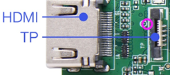 |
| 2 | GND | Ground | Ground | |
| 3 | RST | Input/Output | Reset | |
| 4 | INT | Input/Output | Interrupt | |
| 5 | GND | Ground | Ground | |
| 6 | SCL | Input/Output | I2C Clock | |
| 7 | SDA | Input/Output | I2C Data | |
| 8 | VCC | power supply | 3.3V output | |
| 9 | GND | Ground | Ground | |
| 10 | GND | Ground | Ground | |
Warning
- The board supports TP screens connected to the I2C interface. Please confirm whether the touch screen interface is I2C or USB before connecting.
- The I2C, RST, and INT levels in the interface are 3.3V. If you connect a 1.8V touch screen, you need to do a good job of level conversion.
- Before connecting, please pay attention to whether the electrical definition of the line sequence matches. The touch screen must be connected before powering on. It is not allowed to plug and unplug with power on.
3.2.7 MIPI interface (40pin/0.5mm)
(1) Functional description:
The board supports TP screen connected to I2C interface, and the interface is in the form of 10pin 0.5mm pitch vertical FPC socket.
(2) Electrical definition:
| Serial number | definition | property | describe | |
|---|---|---|---|---|
| 1 | VDD_1V8 | power supply | 1.8V input | 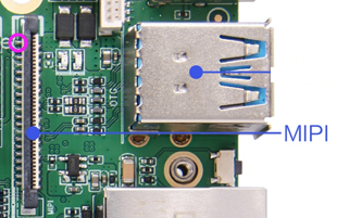 |
| 2 | VDD_3V3 | power supply | 3.3V input | |
| 3 | VDD_3V3 | power supply | ||
| 4 | NC | NC | NC | |
| 5 | Reset | Output | Screen reset signal, high level 3.3V | |
| 6 | NC | NC | NC | |
| 7 | GND | Ground | Ground | |
| 8 | MIPI_D0N | Output | MIPI Port Lane 0 negative output | |
| 9 | MIPI_D0P | Output | MIPI Port Lane 0 positive output | |
| 10 | GND | Ground | Ground | |
| 11 | MIPI_D1N | Output | MIPI Port Lane 1 negative output | |
| 12 | MIPI_D1P | Output | MIPI Port Lane 1 positive output | |
| 13 | GND | Ground | Ground | |
| 14 | MIPI_CKN | Output | MIPI Port clock negative output | |
| 15 | MIPI_CKP | Output | MIPI Port clock positive output | |
| 16 | GND | Ground | Ground | |
| 17 | MIPI_D2N | Output | MIPI Port Lane 2 negative output | |
| 18 | MIPI_D2P | Output | MIPI Port Lane 2 positive output | |
| 19 | GND | Ground | Ground | |
| 20 | MIPI_D3N | Output | MIPI Port Lane 3 negative output | |
| 21 | MIPI_D3P | Output | MIPI Port Lane 3 positive output | |
| 22 | GND | Ground | Ground | |
| 23 | NC | NC | NC | |
| 24 | NC | NC | NC | |
| 25 | GND | Ground | Ground | |
| 26 | NC | NC | NC | |
| 27 | NC | NC | NC | |
| 28 | NC | NC | NC | |
| 29 | NC | NC | NC | |
| 30 | GND | Ground | Ground | |
| 31 | LED- | power supply | LCD Backlight Power Supply - | |
| 32 | LED- | power supply | ||
| 33 | NC | NC | NC | |
| 34 | NC | NC | NC | |
| 35 | NC | NC | NC | |
| 36 | NC | NC | NC | |
| 37 | NC | NC | NC | |
| 38 | NC | NC | NC | |
| 39 | LED+ | power supply | LCD Backlight Power Supply + | |
| 40 | LED+ | power supply | ||
Warning
- The default current setting is 40mA.
3.2.8 MIPI Camera Interface (22pin/0.5mm)
(1) Functional description:
The board supports 1-way mipi camera input, and the interface is a 22-pin 0.5mm pitch vertical FPC socket.
(2) Electrical definition:
| Serial number | definition | property | describe | |
|---|---|---|---|---|
| 1 | GND | Ground | Ground | 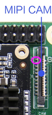 |
| 2 | D0N | Input/Output | mipi data channel 0 negative | |
| 3 | D0P | Input/Output | mipi data channel 0 positive | |
| 4 | GND | Ground | Ground | |
| 5 | D1N | Input/Output | mipi data channel 1 negative | |
| 6 | D1P | Input/Output | mipi data channel 1 positive | |
| 7 | GND | Ground | Ground | |
| 8 | CLKN | Input/Output | mipi clock channel negative | |
| 9 | CLKP | Input/Output | mipi clock channel positive | |
| 10 | GND | Ground | Ground | |
| 11 | D2N | Input/Output | mipi data channel 2 negative | |
| 12 | D2P | Input/Output | mipi data channel 2 positive | |
| 13 | GND | Ground | Ground | |
| 14 | D3N | Input/Output | mipi data channel 3 negative | |
| 15 | D3P | Input/Output | mipi data channel 3 positive | |
| 16 | GND | Ground | Ground | |
| 17 | PWREN | Output | Power-on control | |
| 18 | GPIO | Output | Reserved IO, undefined | |
| 19 | GND | Ground | Ground | |
| 20 | SCL | Output | SCL signal | |
| 21 | SDA | Input/Output | SDA signal | |
| 22 | VDD | power supply | 3.3V output | |
Warning
- The maximum supported resolution is: 940W.
- The signal level of I2C and RST in the interface is 1.8V. If you connect a module with a 3.3V level, you need to do a good job of level conversion.
- Before connecting, please pay attention to whether the electrical definition of the line sequence matches. You need to connect the module first and then power it on. It is not allowed to plug and unplug it while it is powered on.
3.2.9 EDP interface (30pin/0.5mm, back)
(1) Functional description:
Supports the interface for accessing the EDP screen, the interface is in the form of a 30pin 0.5mm pitch FPC socket.
(2) Electrical definition:
| Serial number | definition | property | describe | |
|---|---|---|---|---|
| 1 | NC | -- | Alley-oop | 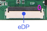 |
| 2 | GND | Ground | Ground | |
| 3 | D1- | Output | Display Port Lane 1 negative output | |
| 4 | D1+ | Output | Display Port Lane 1 positive output interrupted | |
| 5 | GND | Ground | Ground | |
| 6 | D0+ | Output | Display Port Lane 0 negative output | |
| 7 | D0- | Output | Display Port Lane 0 positive output | |
| 8 | GND | Ground | Ground | |
| 9 | AUX+ | Output | Display Port AUX+ chanenl positive singal | |
| 10 | AUX- | Output | Display Port AUX- chanenl negative singal | |
| 11 | GND | Ground | Ground | |
| 12 | PVCC | power supply | eDP LCD screen power output 3.3V | |
| 13 | PVCC | power supply | eDP LCD screen power output 3.3V | |
| 14 | NC | - | Alley-oop | |
| 15 | GND | Ground | Ground | |
| 16 | GND | Ground | Ground | |
| 17 | eDP_HPD | enter | Screen hot-swap detection signal, screen output | |
| 18 | GND | Ground | Ground | |
| 19 | GND | Ground | Ground | |
| 20 | GND | Ground | Ground | |
| 21 | GND | Ground | Ground | |
| 22 | BL-EN | Output | Backlight enable control | |
| 23 | BL-PWM | Output | Backlight brightness pwm control | |
| 24 | NC | -- | Alley-oop | |
| 25 | NC | -- | Alley-oop | |
| 26 | VLED | power supply | 5V output | |
| 27 | VLED | power supply | 5V output | |
| 28 | VLED | power supply | 5V output | |
| 29 | VLED | power supply | 5V output | |
| 30 | NC | -- | Alley-oop | |
3.2.10 IO interface (40pin/2.54mm)
(1) Functional description:
IO is used to provide control signal input/output to peripherals. The voltage level is 3.3V. IO can be connected to Raspberry Pi peripherals.
(2) Electrical definition:
| Serial number | definition | property | describe | |
|---|---|---|---|---|
| 1 | 3V3 | power supply | 3.3V output | 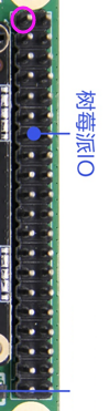 |
| 2 | 5V | power supply | 5V output | |
| 3 | SDA | Input/Output | I2C3_SDA signal | |
| 4 | 5V | power supply | 5V output | |
| 5 | SCL | Input/Output | I2C3_SCL signal | |
| 6 | GND | Ground | Ground | |
| 7 | GPIO | Input/Output | GPIO4_D2 | |
| 8 | TX | Output | TTL-TX3 | |
| 9 | GND | Ground | Ground | |
| 10 | RX | enter | TTL-RX3 | |
| 11 | GPIO | Input/Output | GPIO1_B0 | |
| 12 | GPIO | Input/Output | IO_PWM0_M0 | |
| 13 | GPIO | Input/Output | GPIO1_B1 | |
| 14 | GND | Ground | Ground | |
| 15 | GPIO | Input/Output | GPIO0_A1 | |
| 16 | GPIO | Input/Output | GPIO1_B2 | |
| 17 | 3V3 | Output | 3.3V output | |
| 18 | GPIO | Input/Output | GPIO2_D7 | |
| 19 | MOSI | enter | SPI_MOSI signal | |
| 20 | GND | Ground | Ground | |
| 21 | MISO | Output | SPI_MISO signal | |
| 22 | GPIO | Input/Output | GPIO3_B1 | |
| 23 | SCLK | Output | SPI_CLK signal | |
| 24 | CE0 | Output | SPI_CS0 signal | |
| 25 | GND | Ground | Ground | |
| 26 | CE1 | Output | SPI_CS1 signal | |
| 27 | GPIO | Input/Output | I2C5_SDA | |
| 28 | GPIO | Input/Output | I2C5_SCL | |
| 29 | GPIO | Input/Output | GPIO0_C5 | |
| 30 | GND | Ground | Ground | |
| 31 | GPIO | Input/Output | IO1_5 | |
| 32 | PWM0 | Output | PWM signal | |
| 33 | PWM1 | Output | PWM signal | |
| 34 | GND | Ground | Ground | |
| 35 | GPIO | Input/Output | IO1_1 | |
| 36 | GPIO | Input/Output | GPIO3_C5 | |
| 37 | GPIO | Input/Output | IO1_2 | |
| 38 | GPIO | Input/Output | IO1_3 | |
| 39 | GND | Ground | Ground | |
| 40 | GPIO | Input/Output | IO1_4 | |
Warning
- The IO level of the peripheral device cannot be higher than 3.3V. If the IO level of the docking device is higher than 3.3V, an isolation circuit or a level conversion circuit is required, otherwise the main control and the device will be burned out;
- When using the IO port, pay attention to whether the IO port is input or output;
- Pay attention to the serial power supply of the peripheral device through this IO port (when the power is off, use a multimeter to measure this IO, it should be 0V).
3.2.11 POE interface (2pin/2.0mmX2 pin)
(1) Functional description:
This interface can be connected to an external POE board.
(2) Electrical definition:
| Serial number | definition | property | describe | |
|---|---|---|---|---|
| 1 | GND1(3-6) | enter | Common tap of RJ45_pair3-6 | 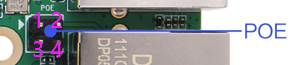 |
| 2 | 48V1(1-2) | enter | Common tap of RJ45_pair1-2 | |
| 3 | GND2(7-8) | enter | Common tap of RJ45_pair7-8 | |
| 4 | 48V2(4-5) | enter | Common tap of RJ45_pair4-5 | |
Warning
- There are standard POE and non-standard POE in the POE power supply market (the difference is that the standard POE power supply uses 1-2-3-6 four-cores to transmit data and current at the same time; non-standard POE uses 1-2-3-6 to transmit data and 4-5-7-8 to transmit current). If you choose a non-standard POE module, it cannot be adapted to the switch power supply equipment of the standard POE; if you choose a standard POE module, you can adapt to the power supply input of the non-standard POE;
- It is recommended that the external POE module should support the IEEE802.3af/at standard. You can ask FAE for the corresponding model specifications;
- The board supports a maximum power input of 30W. If the board has many external high-power peripherals, it is recommended to draw power from the DC socket.
3.3 Other standard interfaces and functions
| interface | standard | Parameter Description |
|---|---|---|
| Storage Interface | TF card | Adopts SD3.0 interface specification, supports up to Class10,minimum write/read speed is 10MB/s, and the maximum capacity can support 128GB |
| USB TYPE-A | USB 2.0, supports up to 480Mbps/s transfer rate (60MB/s) USB 3.0, supports up to 5.0Gbps/s transfer rate (500MB/s) | |
| Ethernet interface | RJ45 connector | Support 10/100/1000M wired network |
| HDMI interface | HDMI TYPE-A | HDMI 1.4, 2.0; supports multiple resolutions, 1920x1080, 1280x720, 720x576, 720x480, etc. |
| Headphone jack | 3.5mm | Support left and right dual channels, support MIC recording |
Chapter 4 Electrical Performance
| project | Minimum | typical | maximum | |
|---|---|---|---|---|
| Power parameters | Voltage | -- | 5V | -- |
| Ripple | -- | -- | 50mV | |
| Current | 3A | |||
| Power supply current (HDMI output, no other peripherals connected) | Working current | 500mA | 1200mA | |
| Standby current | 300mA | 450mA | ||
| Total output | Current | -- | -- | 3A |
| environment | Relative humidity | -- | -- | 80% |
| Operating temperature | 0℃ | -- | 60℃ | |
| Storage temperature | -40℃ | 80℃ | ||
Chapter 5 Minimum Test Items for the Whole Machine
Description:
| Minimum test items for overall stability and reliability | ||
|---|---|---|
| Serial number | Test items | Test Detailed Description |
| 1 | Basic functional performance test | Test the main functional performance of the whole machine, test WiFI, Bluetooth, Ethernet, USB, serial port, video playback and other functions |
| 2 | Software upgrade function test | Verify the upgrade function of the whole product, and test whether the product line flash, USB flash drive upgrade, and network remote upgrade functions are normal. |
| 3 | High temperature aging test | Test the high temperature resistance of the whole machine. After playing the aging work video in a 60℃ environment for 3 days, it can run normally without freezing, abnormal picture, black screen and other electrical problems. |
| 4 | Low temperature power failure test | Test the low temperature resistance of the whole machine. After playing the aging work video in a 0℃ environment for 3 days, it can run normally without freezing, abnormal picture, black screen and other electrical problems. |
| 5 | Short-time timing switch at room temperature | Test the product's ability to withstand power on and off, program it to shut down in 3 minutes and start up in 7 minutes, and run normally after 7 days of operation without electrical failures such as freezing, abnormal images, black screen, etc. The probability of abnormal records does not exceed 4/10000. |
| 6 | Electrostatic Discharge (ESD) Test | The simulation test evaluates the product's ability to defend against electrostatic discharge. According to the IEC 61000-4-2 test standard, the product is subjected to ±4KV contact and ±8KV air discharge. The product must meet the A or B level judgment to be accepted. C and D levels are considered unqualified. |
| 7 | Sweep frequency vibration test | Test the product's vibration resistance to see if it has passed the simulated transportation test and the board solder and parts' bearing capacity to avoid potential problems. Use a vibration tester to test the product. After the test, if the test product has no looseness or fall-off in structure and can operate normally, and has no electrical defects such as freezing, abnormal picture, black screen, and structural appearance damage, it is judged as OK. |
| 8 | Free drop test | The simulated transport and handling product's ability to withstand a drop is used to determine the bearing capacity of the machine mechanism to avoid potential problems and improve the design and process. After the test is completed, the test product can operate normally without freezing, abnormal images, black screens, and other electrical defects and structural appearance damage. It is judged to be OK |
| 9 | Short-time power-off shock at room temperature | This test is used to test the product's ability to withstand power on and off. |
| 10 | Normal temperature long time timer switch | Verify the stability of the MCU and the stability of the system. The timer power on/off tool is set to start at 9:30 am and shut down at 18:30. The log records the time interval between each startup and shutdown. If the error is less than 1 minute, it is considered qualified. |
| 11 | Voltage overvoltage and undervoltage test | According to the power supply specifications of the Android board, the voltage tolerance of the board is tested through voltage changes. The whole machine is tested for 2 hours at -20% +30% of the rated power supply. During and after the test, if the test product can operate normally without freezing, abnormal images, black screen and other electrical problems, it is judged as OK. |
Chapter 6 Configurable Parameters Table (Differences)

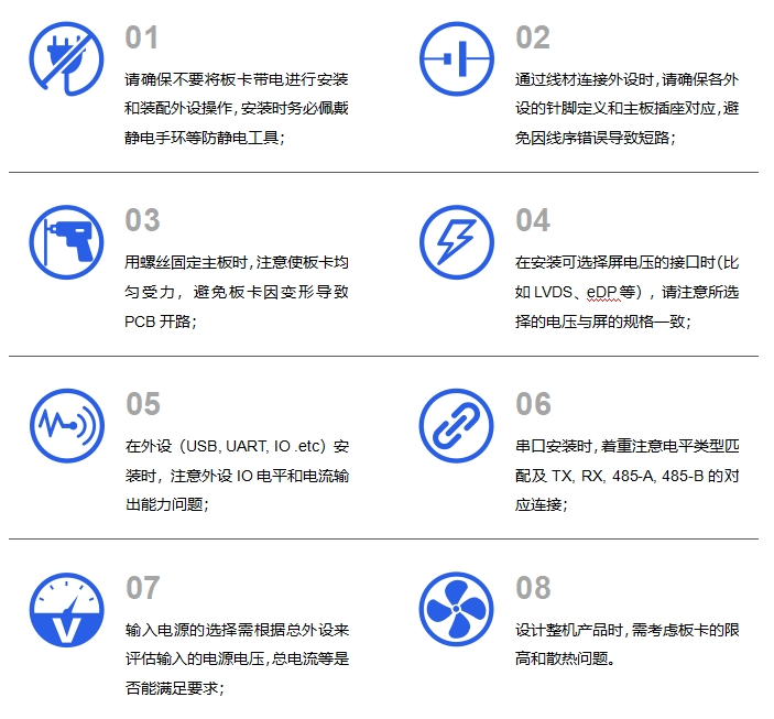
Chapter 7 Precautions for use (must read)
Copyright Notice
This user manual, including but not limited to all the information contained therein, is protected by copyright law. Without the permission of ShiMetaPi, no imitation, copying, excerpting, translating, distributing or other use of the information is allowed.
Disclaimer
The ownership and intellectual property rights of third-party product names or contents mentioned in this user manual belong to the respective product or content owners and are protected by current intellectual property laws and international treaties.