15 M.2 SSD
1 M.2 Interface Introduction
The M.2 interface is a physical interface standard that can support multiple different communication protocols, including:
- PCIe (Peripheral Component Interconnect Express)
- SATA (Serial Advanced Technology Attachment)
- USB (Universal Serial Bus)
Therefore, the speed and performance of the M.2 interface depend on the communication protocol and hardware implementation used. The M.2 interface can support PCIe 3.0, which is a high-speed data transmission protocol, usually used to connect graphics cards, solid-state drives (SSDs), and other devices requiring high bandwidth.
In modern computers, especially in the consumer market, the most common and important application of the M.2 interface is connecting solid-state drives (SSDs). And what we usually call "M.2 SSD", according to different protocols, is mainly divided into two categories:
- NVMe protocol with higher performance (running on PCIe bus)
- SATA protocol with performance comparable to traditional SATA hard drives
Simple understanding M.2 is the "slot and appearance", PCIe is the "highway", SATA is the "regular road", and NVMe is the "super traffic rules" running on the highway. Through this M.2 physical interface, we can choose which "road" and which "rules" the hard drive uses.
1.1 M.2 Slot Specifications
M.2 slots come in different physical sizes, including:
- 2242
- 2260
- 2280
- 22110
These numbers represent the length and width of the slot.
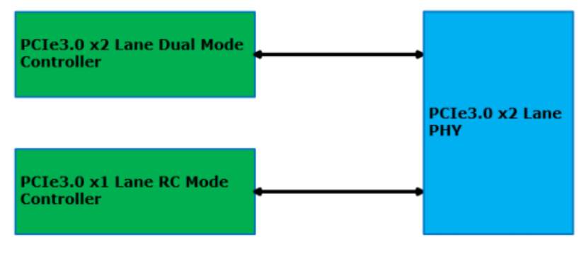
1.2 RK3568 PCIe Architecture
The RK3568 chip has:
- 1 PCIe3.0 x2 Lane Dual Mode controller
- 1 PCIe3.0 x1 Lane RC Mode controller
- 1 PCIe3.0 x2 Lane PHY
Both the PCIe3.0 x2 Lane Dual Mode controller and the PCIe3.0 x1 Lane RC Mode controller are connected to the PCIe3.0 x2 Lane PHY, meaning two controllers connect to the same PHY.
The connection diagram is as follows:
2 M.2 Interface Board Card Location
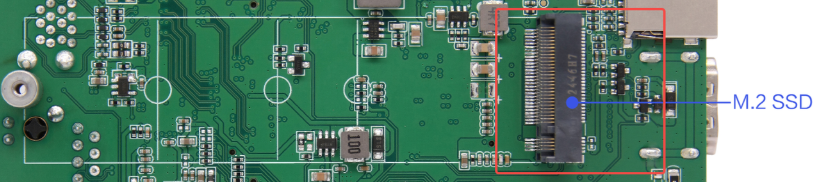
The M.2 interface specifications of the development board:
- PCIe type: PCIe Gen3 x 2 lane
- Length specification: 2280
- Protocol support: This interface can only be used with M2 NVMe protocol solid-state drives
3 M.2 SSD Usage - Command Line Method
3.1 Device Tree File Explanation
Tips
The file path below: out/kernel/src_tmp/linux-5.10/arch/arm64/boot/dts/rockchip Need to compile the source code first.
The pins used by PCIe are dedicated pins. You only need to enable the corresponding controller, and the corresponding pins will be set to the corresponding mode.
Tips
Although this part of DTS code is long, there are few places that users need to modify, mainly changing the status attribute to okay. Therefore, this chapter does not provide detailed analysis of the DTS, only showing key code and brief explanations!
First, let's look at the basic definition layer (rk3568.dtsi). Due to limited space, only the code for pcie30phy and pcie3x2 nodes is shown. Other nodes only have different register addresses and PHY usage.
pcie30phy: phy@fe8c0000 {
        compatible = "rockchip,rk3568-pcie3-phy";
        reg = <0x0 0xfe8c0000 0x0 0x20000>;
        #phy-cells = <0>;
        clocks = <&pmucru CLK_PCIE30PHY_REF_M>, <&pmucru CLK_PCIE30PHY_REF_N>,
                 <&cru PCLK_PCIE30PHY>;
        clock-names = "refclk_m", "refclk_n", "pclk";
        resets = <&cru SRST_PCIE30PHY>;
        reset-names = "phy";
        rockchip,phy-grf = <&pcie30_phy_grf>;
        status = "disabled";
};

pcie3x2: pcie@fe280000 {
        compatible = "rockchip,rk3568-pcie", "snps,dw-pcie";
        #address-cells = <3>;
        #size-cells = <2>;
        bus-range = <0x20 0x2f>;
        clocks = <&cru ACLK_PCIE30X2_MST>, <&cru ACLK_PCIE30X2_SLV>,
                 <&cru ACLK_PCIE30X2_DBI>, <&cru PCLK_PCIE30X2>,
                 <&cru CLK_PCIE30X2_AUX_NDFT>;
        clock-names = "aclk_mst", "aclk_slv",
                      "aclk_dbi", "pclk", "aux";
        device_type = "pci";
        interrupts = <GIC_SPI 165 IRQ_TYPE_LEVEL_HIGH>,
                     <GIC_SPI 164 IRQ_TYPE_LEVEL_HIGH>,
                     <GIC_SPI 163 IRQ_TYPE_LEVEL_HIGH>,
                     <GIC_SPI 162 IRQ_TYPE_LEVEL_HIGH>,
                     <GIC_SPI 161 IRQ_TYPE_LEVEL_HIGH>;
        interrupt-names = "sys", "pmc", "msg", "legacy", "err";
        #interrupt-cells = <1>;
        interrupt-map-mask = <0 0 0 7>;
        interrupt-map = <0 0 0 1 &pcie3x2_intc 0>,
                        <0 0 0 2 &pcie3x2_intc 1>,
                        <0 0 0 3 &pcie3x2_intc 2>,
                        <0 0 0 4 &pcie3x2_intc 3>;
        linux,pci-domain = <2>;
        num-ib-windows = <6>;
        num-ob-windows = <2>;
        max-link-speed = <3>;
        msi-map = <0x2000 &its 0x2000 0x1000>;
        num-lanes = <2>;
        phys = <&pcie30phy>;
        phy-names = "pcie-phy";
        power-domains = <&power RK3568_PD_PIPE>;
        ranges = <0x00000800 0x0 0x80000000 0x3 0x80000000 0x0 0x800000
                  0x81000000 0x0 0x80800000 0x3 0x80800000 0x0 0x100000
                  0x83000000 0x0 0x80900000 0x3 0x80900000 0x0 0x3f700000>;
        reg = <0x3 0xc0800000 0x0 0x400000>,
              <0x0 0xfe280000 0x0 0x10000>;
        reg-names = "pcie-dbi", "pcie-apb";
        resets = <&cru SRST_PCIE30X2_POWERUP>;
        reset-names = "pipe";
        /* rockchip,bifurcation; lane0 when using 1+1 */
        status = "disabled";

        pcie3x2_intc: legacy-interrupt-controller {
                interrupt-controller;
                #address-cells = <0>;
                #interrupt-cells = <1>;
                interrupt-parent = <&gic>;
                interrupts = <GIC_SPI 162 IRQ_TYPE_EDGE_RISING>;
        };
};
The above is the code for the pcie3x2 node. The three PCIE controllers provided by rk3568 are:
- pcie2x1: PCIe 2.0 single-lane controller, register address 0xfe260000, uses combphy2_psq as PHY
- pcie3x1: PCIe 3.0 single-lane controller, register address 0xfe270000, uses pcie30phy as PHY, supports bifurcation mode
- pcie3x2: PCIe 3.0 dual-lane controller, register address 0xfe280000, uses pcie30phy as PHY, supports bifurcation mode
Each controller is configured with corresponding clock sources, interrupts, power domains, and reset signals. The default state is disabled.
Next is the pin configuration layer (rk3568-pinctrl.dtsi):
pcie20m0_pins: pcie20m0-pins {
	rockchip,pins =
		/* pcie20_clkreqnm0 */
		<0 RK_PA5 3 &pcfg_pull_none>,
		/* pcie20_perstnm0 */
		<0 RK_PB6 3 &pcfg_pull_none>,
		/* pcie20_wakenm0 */
		<0 RK_PB5 3 &pcfg_pull_none>;
};

pcie30x1m0_pins: pcie30x1m0-pins {
	rockchip,pins =
		/* pcie30x1_clkreqnm0 */
		<0 RK_PA4 3 &pcfg_pull_none>,
		/* pcie30x1_perstnm0 */
		<0 RK_PC3 3 &pcfg_pull_none>,
		/* pcie30x1_wakenm0 */
		<0 RK_PC2 3 &pcfg_pull_none>;
};

pcie30x2m0_pins: pcie30x2m0-pins {
	rockchip,pins =
		/* pcie30x2_clkreqnm0 */
		<0 RK_PA6 2 &pcfg_pull_none>,
		/* pcie30x2_perstnm0 */
		<0 RK_PC6 3 &pcfg_pull_none>,
		/* pcie30x2_wakenm0 */
		<0 RK_PC5 3 &pcfg_pull_none>;
};
Each PCIE controller provides multiple pin multiplexing modes (m0, m1, m2). Each configuration includes three key signals:
- clkreqn: Clock request signal, used for power management
- perstn: Reset signal, used for hardware reset control
- waken: Wake signal, used to wake from low power state
Finally, let's look at the board-level configuration layer (rk3568-evb6-ddr3-v10.dtsi)
&pcie30phy {
	status = "okay";
};

&pcie2x1 {
	reset-gpios = <&gpio1 RK_PB2 GPIO_ACTIVE_HIGH>;
	vpcie3v3-supply = <&pcie20_3v3>;
	status = "okay";
};

&pcie3x1 {
	rockchip,bifurcation;
	reset-gpios = <&gpio3 RK_PA1 GPIO_ACTIVE_HIGH>;
	vpcie3v3-supply = <&pcie30_3v3>;
	status = "okay";
};

&pcie3x2 {
	rockchip,bifurcation;
	reset-gpios = <&gpio2 RK_PD6 GPIO_ACTIVE_HIGH>;
	vpcie3v3-supply = <&pcie30_3v3>;
	status = "okay";
};- Enable PHY: Set &pcie30phy node status = "okay" to enable PCIe 3.0 PHY
- Configure reset GPIO: Specify reset control pin through reset-gpios attribute
- Configure power supply: Associate 3.3V power regulator through vpcie3v3-supply attribute
- Enable bifurcation mode: For PCIe 3.0 controller, can enable lane bifurcation function through rockchip,bifurcation attribute
- Enable controller: Set status = "okay" to enable corresponding PCIE controller
Caution
Unlike TF cards, SSDs do not support hot-plugging! Please ensure the system is turned off before installing the solid-state drive to avoid data loss.
Users need to install the solid-state drive while the power is off, then start the system.
3.2 Common Commands for Testing M.2 SSD
After installing the drive, you can use commands just like with TF cards.
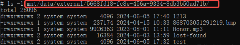
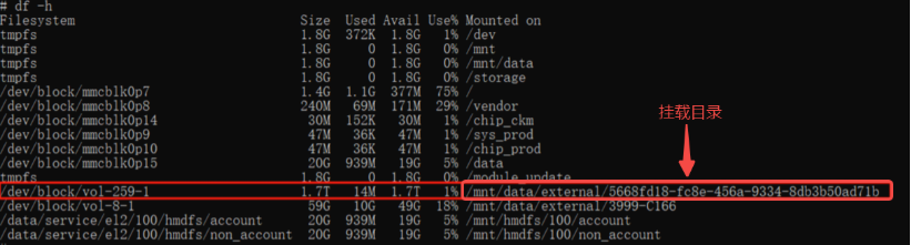
Use the command below to view the mount directory. After entering the mount directory, you can view files and operate through the command line.
df -h3.3 Specific Demonstration of M.2 SSD Usage
View mount directory:
View SSD content: