18 Camera
1 Camera Introduction
In modern society, with the improvement of chip computing power and AI empowerment, cameras, as almost essential sensors for mid-to-high-end embedded devices, are undergoing continuous innovation and performance optimization.
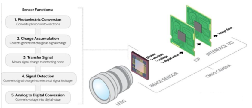
Below is the composition structure diagram of a COMS sensor camera, roughly divided into lens, image sensor, and image processing unit. The following will explain based on the author's understanding.
1.1 Introduction to Lens
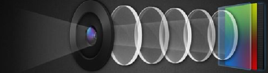
Let's first introduce the lens, as shown in the figure above, it is composed of multiple lenses. In theory, only one lens is needed for imaging, but there are problems like chromatic aberration and astigmatism. Using multiple lens combinations can effectively correct aberrations. In addition, by changing the position of multiple lenses, zoom can be achieved. Of course, the most important point is that focusing for most cameras is also achieved by changing the position of the lens group.
Cameras that support zoom and auto-focus generally have a micro motor to change the position of the lens. The common camera motor type is VCM (Voice Coil Motor). The structure diagram is as follows:
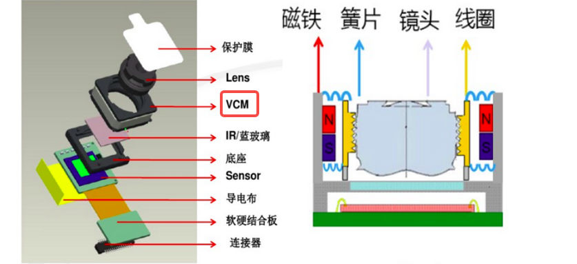
When the coil is energized, a magnetic field is generated. By adjusting the current flowing through the magnetic field, the forward and backward movement of the lens can be achieved. This structure is called VCM (Voice Coil Motor).
1.2 Introduction to CMOS Sensor
Let's briefly talk about the most important part of the camera - the image sensor, which is what everyone calls CMOS. The function of CMOS is to absorb photoelectrons, so that each pixel can accumulate different amounts of charge. These collected charges are converted into corresponding intensity voltage signals by the amplifier under each pixel. The voltage signal, as an analog quantity, is converted to digital signal through ADC. Taking 12-bit ADC as an example, each pixel is divided into 4096 levels according to brightness. At this point, a raw file of a black and white image can be obtained.
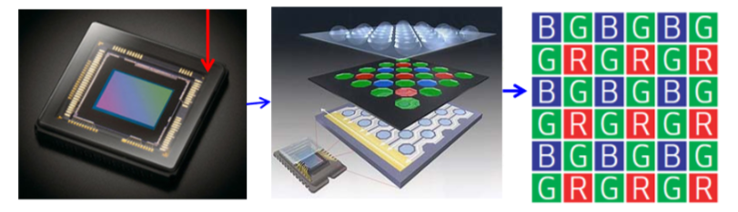
Add a color filter in front of each pixel. For example, a green filter only allows green light to pass. Then the light intensity value of this point is the brightness level of green light. The entire digital grid described by the brightness levels of RGB three primary colors is the camera's raw file.
At this point, friends understand why when we use our phones to take photos at night, we need to wait a few seconds after clicking the shutter to complete, while during the day it's fast. This is because we need to wait for the CMOS unit to collect more photoelectrons, otherwise we get an all-black image. For friends with photography basics, you also know the origin of the three elements of photography (aperture, shutter, ISO), all of which control the amount of light in different ways!
1.3 Introduction to Image Processing Unit
The image processing unit ISP processes the raw file. It estimates the true color of each pixel based on the value of each pixel through algorithms (for example, if it finds the red pixel (R) value on the left is 50, and the red pixel value on the right is 55. Then it will reasonably infer: "Hmm, the red value at this position is probably around 52"). After algorithm processing, a color image is born. If you need to output images in formats like JPG, the processor performs white balance correction, sharpening, noise reduction, and compression on the raw file to finally generate the image we need.
2 Camera Interface Location in Board Card
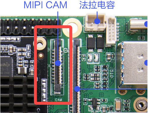
The board reserves one MIPI camera interface. Currently, it has adapted to two cameras: GC8034 from GalaxyCore and OV5695 from OmniVision.
The specific parameters can be found in the table below:
| Parameter | GC8034 | OV5695 |
|---|---|---|
| Manufacturer | China GalaxyCore (GalaxyCore) | USA OmniVision (OmniVision) |
| Resolution | 3264H x 2448V (~8 megapixels) | 2592H x 1944V (~5 megapixels) |
| Optical Size | 1/4 inch | 1/4 inch |
| Output Format | RAW10 / RAW8 | 10-bit RGB RAW |
| Interface | MIPI (supports 2 lane or 4 lane) | MIPI (supports 1 lane or 2 lane) |
| Frame Rate | 30fps at full size (MIPI 4 lane) | 30fps at full size (5MP) |
3 Camera Testing
3.1 Device Tree Details
Tips
The file path below: out/kernel/src_tmp/linux-5.10/arch/arm64/boot/dts/rockchip
Need to compile the source code first.
Since the camera device tree configuration is complex, according to the SDK's camera configuration, the data transmission process is roughly divided into the following stages:
Camera Data Transmission Process:
| Step | Component/Stage | Function Description | Data Flow |
|---|---|---|---|
| 1 | Camera Module | Image sensor captures light signal | Light signal → electrical signal |
| 2 | I2C Control Configuration | Configure camera parameters | Control signal transmission |
| 3 | Image Data Acquisition | Convert electrical signal to digital signal | Analog signal → digital signal |
| 4 | MIPI CSI-2/DVP Interface Transmission | High-speed data interface transmission | Digital image data transmission |
| 5 | CSI2 D-PHY Physical Layer Processing | Physical layer signal processing and synchronization | Signal conditioning and clock recovery |
| 6 | ISP Image Signal Processing | Image quality optimization processing | Raw data → processed data |
| 7 | Noise Reduction, Color Correction, etc. | Image enhancement and correction | Image quality improvement |
| 8 | Data Output | Processed image data | Final image data |
| 9 | Storage to Memory | Data caching and storage | Memory write |
| 10 | Display | Image display output | Screen display |
Since the camera device tree configuration is complex, it is not detailed here.
In the i2c4 node of the board-level matching file rk3568-toybrick-x10.dtsi, excerpts of gc8034 and ov5695 are given as examples:
&i2c4 {
    status = "okay";                              // Enable I2C4 bus

    gc8034: gc8034@37 {                           // GC8034 camera module, I2C address 0x37
        compatible = "galaxycore,gc8034";         // Compatibility string, for driver matching
        reg = <0x37>;                             // I2C device address
        clocks = <&cru CLK_CIF_OUT>;              // Clock source: CRU's CIF output clock
        clock-names = "xvclk";                    // Clock name: external clock
        power-domains = <&power RK3568_PD_VI>;    // Power domain: video input power domain
        pinctrl-names = "default";                // Pin control state name
        pinctrl-0 = <&cif_clk>;                   // Default pin configuration: CIF clock pin
        reset-gpios = <&gpio0 RK_PD6 GPIO_ACTIVE_LOW>;    // Reset GPIO, low level active
        pwdn-gpios = <&gpio4 RK_PB4 GPIO_ACTIVE_LOW>;     // Power control GPIO, low level active
        rockchip,grf = <&grf>;                    // General register file reference
        rockchip,camera-module-index = <0>;       // Camera module index number
        rockchip,camera-module-facing = "back";   // Camera facing: rear
        rockchip,camera-module-name = "RK-CMK-8M-2-v1";   // Camera module name
        rockchip,camera-module-lens-name = "CK8401";      // Lens name
        port {                                    // Port definition, for connecting other devices
            gc8034_out: endpoint {                // Output endpoint
                remote-endpoint = <&mipi_in_ucam1>;       // Connect to MIPI CSI's ucam1 input
                data-lanes = <1 2 3 4>;           // Use 4 data lanes
            };
        };
    };
}
.....

    ov5695: ov5695@36 {                           // OV5695 camera module, I2C address 0x36
        status = "okay";                          // Enable this device
        compatible = "ovti,ov5695";               // Compatibility string, OmniVision driver
        reg = <0x36>;                             // I2C device address
        clocks = <&cru CLK_CIF_OUT>;              // Clock source: CRU's CIF output clock
        clock-names = "xvclk";                    // External clock name
        power-domains = <&power RK3568_PD_VI>;    // Power domain: video input power domain
        pinctrl-names = "default";                // Pin control state name
        pinctrl-0 = <&cif_clk>;                   // Default pin configuration: CIF clock pin
        reset-gpios = <&gpio0 RK_PD6 GPIO_ACTIVE_LOW>;    // Reset control GPIO, low level active
        pwdn-gpios = <&gpio4 RK_PB4 GPIO_ACTIVE_LOW>;     // Power control GPIO, low level active
        rockchip,camera-module-index = <0>;       // Camera module index number
        rockchip,camera-module-facing = "back";   // Camera facing: rear
        rockchip,camera-module-name = "TongJu";   // Module manufacturer name
        rockchip,camera-module-lens-name = "CHT842-MD";   // Lens model
        port {                                    // Port configuration
            ov5695_out: endpoint {                // Output endpoint
                remote-endpoint = <&mipi_in_ucam2>;       // Connect to MIPI CSI's ucam2 input
                data-lanes = <1 2>;               // Use 2 data lanes
            };
        };
    };
};
3.2 Camera Effect File Description
For cameras that output raw images, the image effect needs to be adjusted through ISP to meet normal requirements. Currently, the M4-R1 effect files are adapted to GC8034 by default. If you need to adapt other raw cameras, you also need to modify the effect files on the board!
Below is an example of adapting ov5695.
After installing the HDC tool, enter in terminal:
# Grant permission to modify system folder
hdc shell mount -o remount,rw /vendor
# Push effect file
hdc file send "C:\Users\Administrator\Documents\ov5695_TongJu_CHT842-MD.json" /vendor/etc/iqfil.json
# Reboot the board
hdc shell reboot
After rebooting, the ISP module on the board will read this json file to make ov5695 output images normally.
Note
The effect file for ov5695 is located at the following path: "M4-R1/05-Development-Materials/01-OpenHarmony-Development-Materials/iqfile"
3.3 Specific Demonstration of Camera Testing
Taking the adapted OV5695 as an example, connect the camera to the MIPI CAM interface while the power is off. Do not hot-plug!!! (The author burned one board and camera this way)
Open the built-in camera application of HarmonyOS:
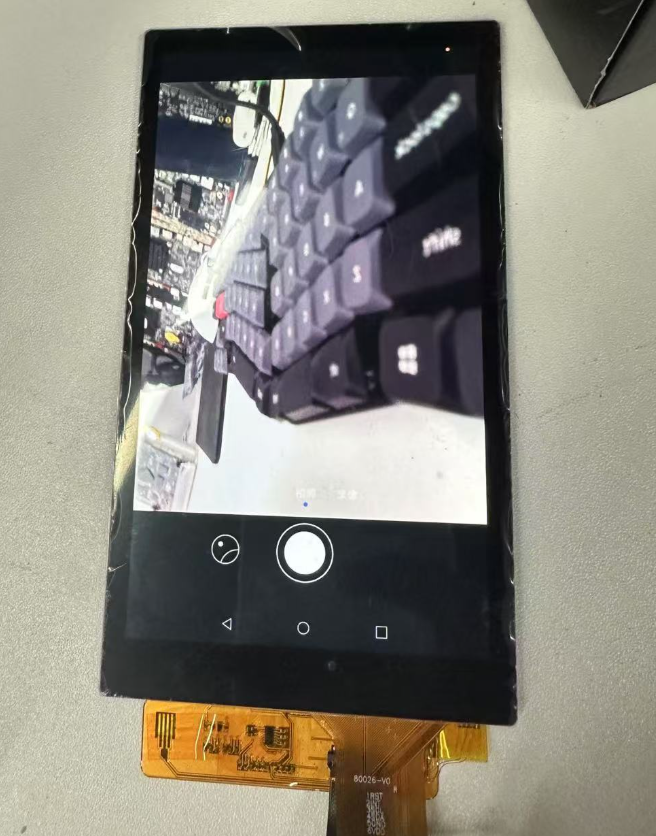
Successfully captured image, testing normal.