FPGA FSPI Communication Demo
1 Demo Introduction
This demo runs a Linux system on the ARM side and performs read/write tests on the FPGA DRAM via the FSPI bus.
2 Communication Flow Between ARM and FPGA
ARM Side Implements SPI Master Function
Open the SPI device node: open the /dev/spidev4.0 device node.
Configure the FSPI bus: use ioctl commands to configure the polarity, phase, communication rate, and data length of the FSPI bus.
Select the transfer mode: you can choose single-wire mode, dual-wire mode, or quad-wire mode. When quad-wire mode is set, both data transmission and reception use quad-wire mode. This demo only supports quad-wire mode.
Data transmission: send data to the FSPI bus and read data from the FSPI bus.
Verify data: verify the transmitted data, then print the read/write speed and bit error rate.
FPGA Side Implements SPI Slave Function
Data storage: the FPGA saves the data sent by the SPI Master to DRAM.
Data read: when the SPI Master initiates a read data request, the FPGA reads data from DRAM and transfers it to the SPI Master via the FSPI bus.
3 Procedure
Open a terminal and copy the executable smdt_spi_rw from the bin directory of this demo (05-开发资料\软件开发资料\linux_demo\smdt_fpga_fspi_demo\bin) to the development board's filesystem (the source code can be found in the src directory).
#修改 Linux 内核日志的显示级别,内核的日志级别被设置为只显示紧急或更高级别的消息
echo 1 4 1 7 > /proc/sys/kernel/printk
In the terminal, run the following commands to switch to the directory containing the smdt_fpga_fspi_demo executable.
#切换到 smdt_spi_rw 可执行程序所在目录
cd ‘可执行文件所在目录’

#查看 smdt_spi_rw 是否在该目录下
ls
If the executable smdt_spi_rw is in the current directory, modify the executable's permissions.
#修改文件权限
chmod 777 smdt_spi_rw

#查询是否修改成功
ls -ld smdt_spi_rw
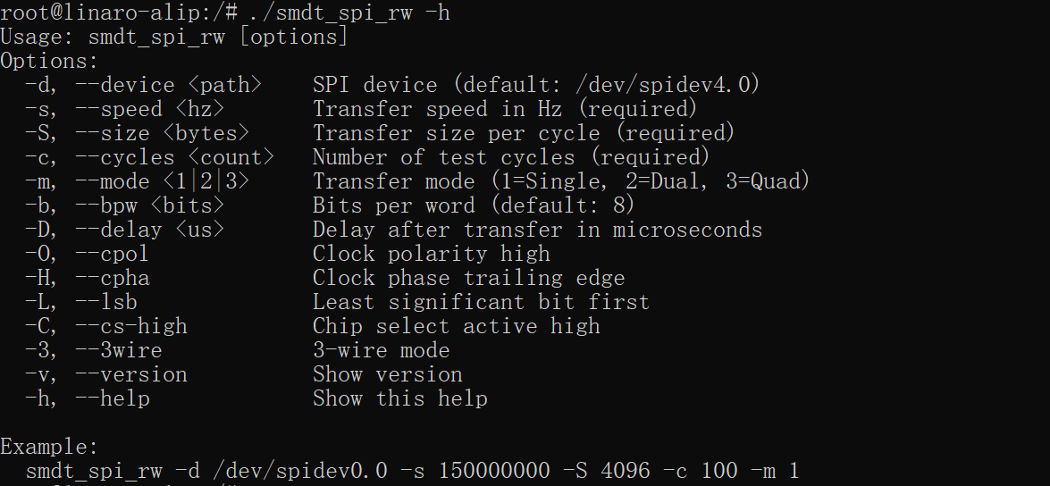
After confirming that the file permissions have been successfully modified, run ./smdt_spi_rw -h to view the program's help information.
#查看帮助信息
./smdt_spi_rw  -h
The execution result is shown in the figure below:
Functional Test
Enter the following command. On the ARM side, 2048 bytes of random data are written to the FPGA's DRAM via the FSPI bus configured in quad-wire mode, then the data is read back for verification. The program prints the FSPI bus read/write speed and the calculated bit error rate. The execution result is shown in the figure below.
./smdt_spi_rw -d /dev/spidev4.0 -s 150000000 -OH -m 3 -S 2048 -c 1

# 参数说明如下:

# `-d`:用于指定设备节点。

# `-s`:用于设置通信时钟的频率,单位是赫兹(Hz)。

# `-O`:表示时钟极性反转,即CPOL(Clock Polarity)设置为1。

# `-H`:表示在时钟周期开始时的第二个边沿采集数据,即CPHA(Clock Phase)设置为1。

# `-m`:选择传输模式,其中1代表单线模式,2代表双线模式,3代表四线模式。

# `-S`:设置传输数据的大小,单位是字节(Byte)。

# `-c`:设置循环传输数据包的次数。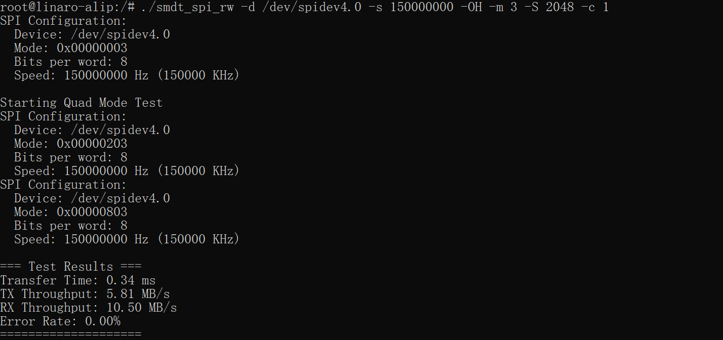
As shown in the figure above, the measured write speed is 5.81 MB/s, the read speed is 10.5 MB/s, and the bit error rate is 0.00%.
Performance Test
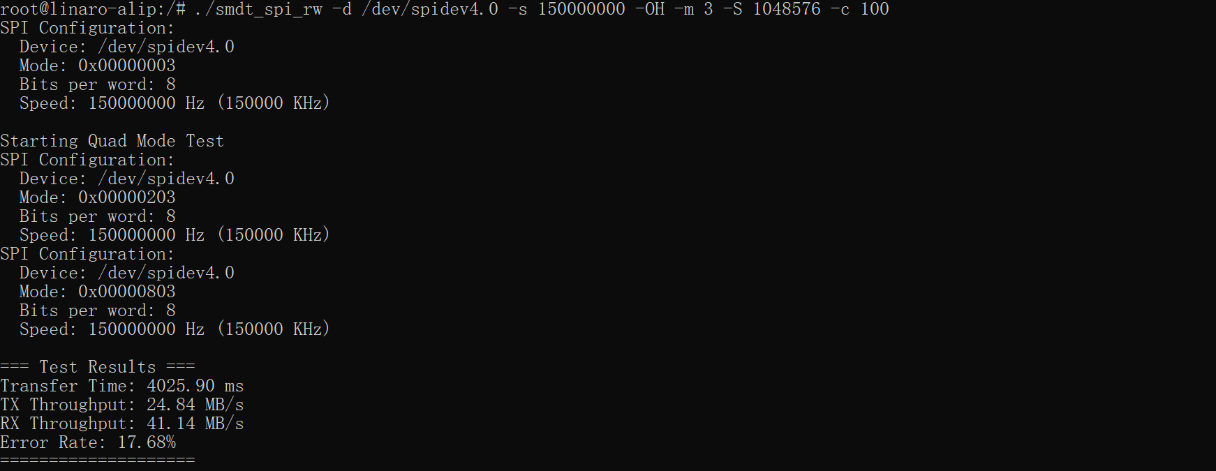
For performance testing, set the FSPI bus communication clock frequency to 150MHz. With this setting, the ARM will write 1MB of random data to the FPGA's DRAM via the FSPI bus, then read the data back, and repeat this process 100 times. Data verification is not performed during the test. The final FSPI bus read/write speed and error rate will be reported. The execution result is shown in the figure below. This demo is designed to read/write 2048 bytes of random data to the FPGA DRAM at a time, so the bit error rate is relatively high.
./smdt_spi_rw -d /dev/spidev4.0 -s 150000000 -OH -m 3 -S 1048576 -c 100