
ARM and FPGA Communication
1 Hardware Interface Introduction
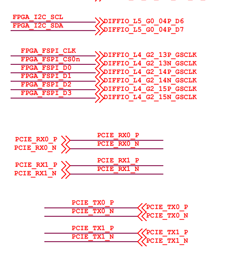
There are three interfaces for FPGA-RK communication: IIC, FSPI, and PCIe. The schematic is shown below:
2 IIC Communication
In IIC communication, the FPGA acts as the slave with the device address 0x66.
Currently, three register addresses are defined in the code: 0x00, 0x01, and 0x02. Among them, 0x02 is a read-only register.
For the 0x00 register, you can test whether the read and written data are correct. For example, write 1, and reading it back should also return 1, which means the communication is normal.
i2cdetect -r -y -a 0
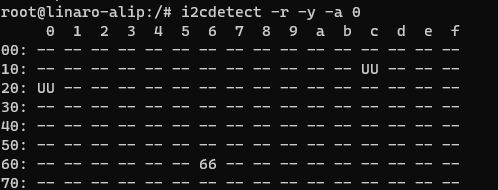
You can see there is a 0x66 address on the I2C bus.
i2cset -r -y -a 0 0x66 0x00 0x40

After running this command, 0x40 is written to the 0x00 register.
Now enter the command i2cdump -f -y -a 0 0x66
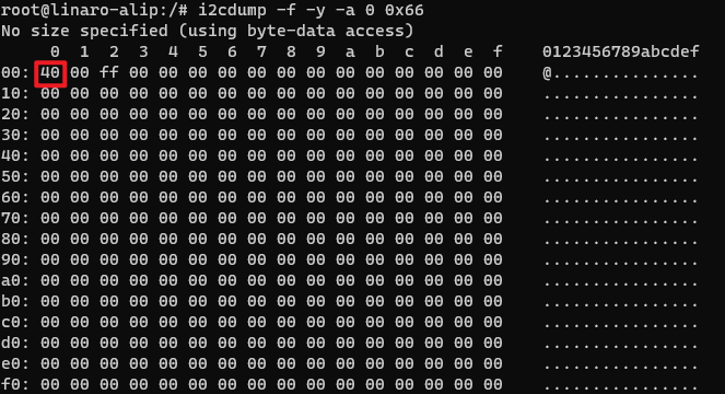
This command lists the values of all registers of 0x66. You can see that the value of register 0x00 is already the 0x40 just written.
i2cget -f -y -a 0 0x66 0x00

Read the value of register 0x00. As you can see, it reads back 0x40, consistent with the written value.
The 0x01 register can control the LED state. Enter the following command:
i2cset -f -y -a 0 0x66 0x01 0x01
Now the LED on the carrier board lights up.
Enter the following command:
i2cset -f -y -a 0 0x66 0x01 0x00
Now the LED on the carrier board turns off.
i2cset -f -y -a 0 0x66 0x01 0x03
Now both LEDs on the carrier board light up.
Because the code assigns the lower 2 bits of this register to the LEDs, the LEDs only light up when the lower 2 bits are 1. At this point, IIC read/write communication is verified as working.
3 FSPI Communication
The FPGA and RK interact via FSPI. The FPGA has a RAM used to buffer data, implementing a read/write loop.
First, load the driver:
insmod smdt_spi_controller.ko

Then enter the command: lsmod

When the text in the red box above appears, it means the driver has been loaded successfully.
Switch the directory to the folder containing the smdt_spi_rw executable, then enter the command:
./smdt_spi_rw -d /dev/spidev4.0 -s 50000000 -OH -m 3 -S 1024 -c 1
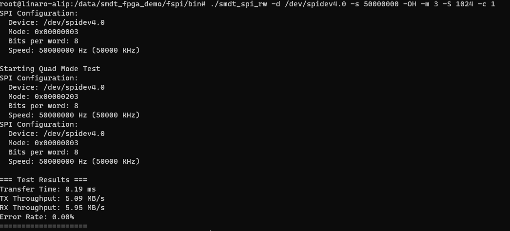
A Byte error rate of 0 means the communication is normal and the data read/write is correct.
Here -s sets the communication frequency, 50MHz.
-m selects the mode: 1 for single-wire mode, 2 for dual-wire mode, and 3 for quad-wire mode.
-S indicates the transfer size, here 1024. Since the FPGA's RAM depth is set to 2048, byte errors will occur once the transfer exceeds 2048.
-c indicates the number of transfers; 1 means transfer once.
4 PCIe Communication
Related file paths
smdt_fpga_dma_memcpy_demo project directory path:01-开发资料(百度云盘) -> 05-开发资料 -> 01-Linux系统 -> linux_demo -> smdt_fpga_dma_memcpy_demo
(Based on the project path above) FPGA flashing-file path: fpga_sfc -> dram_pcie_pg2l50h.sfc smdt_fpga_dma_memcpy_demo executable path: bin -> smdt_dma_memcpy_demo
4.1 Flashing the FPGA Program
The FPGA side needs to be flashed with the PCIe project first, because the RK only detects PCIe devices once during power-up. Therefore, you must ensure that the FPGA has loaded the PCIe program before the RK starts up, otherwise detection will fail.
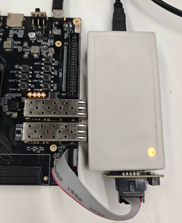
- Connect the FPGA USB downloader properly.
Note
After inserting the USB into the computer's USB port, the downloader lights up red. After the board is powered on, the downloader lights up yellow.
- Open the FPGA flashing software.

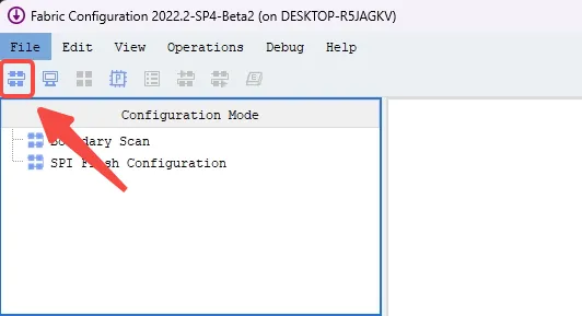
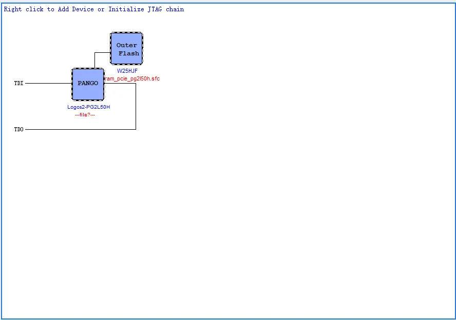
- Power on the development board, then click the icon pointed to by the arrow in the software.
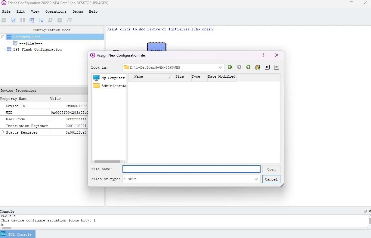
- Once the device is detected, the following interface appears. Close the popup window.
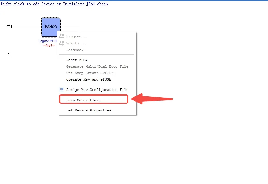
- Move the mouse over the chip, right-click, then select the option pointed to by the arrow in the figure below.
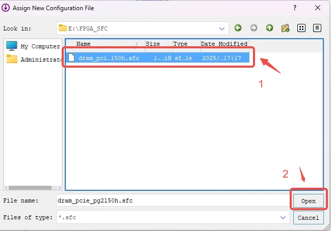
- In the popup window, select the required
dram_pcie_pg2l50h.sfc, then click 【Open】.
Note
The storage path of the sfc file must not contain Chinese characters, otherwise an error will occur and it cannot be opened.
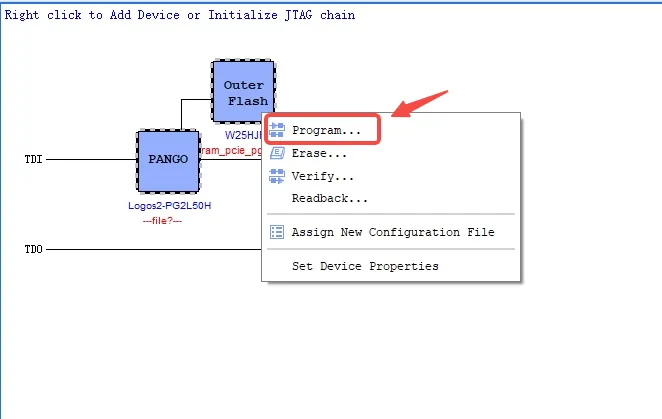
- Right-click 【Outer Flash】 and select the 【Program】 option pointed to by the arrow in the figure below to flash the program.
- Wait for flashing to complete...

- When the Console displays the following information, flashing is complete.

4.2 Running the PCIe Communication Demo
Restart the development board.
In the debug tool, enter the following commands to switch to adb.
echo 1 > /sys/devices/platform/fe8a0000.usb2-phy/otg_mode
echo 2 > /sys/devices/platform/fe8a0000.usb2-phy/otg_mode
usbdevice start
The actual operation is as follows:

- Open cmd and check whether there is an adb device.
adb devices
- Push
smdt_dma_memcpy_demoto the board via theadb pushcommand.
Note
In this example, smdt_dma_memcpy_demo is placed in drive E and will be pushed to the /data directory on the board.
adb push E:\smdt_dma_memcpy_demo /data/
- Check on the board whether the file exists, and add the executable permission. Enter the following commands in cmd.
adb shell
cd /data
ls
chmod +x ./smdt_dma_memcpy_demo
ls -al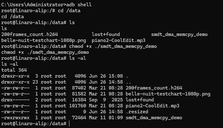
- Use the following commands to check whether PCIe has established a link and whether
input_dev_demohas been generated.
lspci -vv
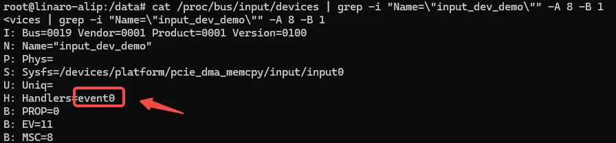
cat /proc/bus/input/devices | grep -i "Name=\"input_dev_demo\"" -A 8 -B 1
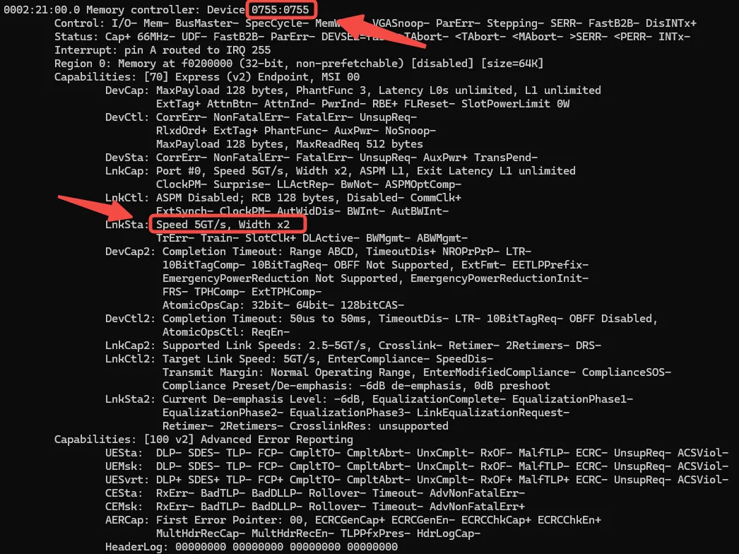
After entering lspci -vv, the output is shown in the figure below. If 0755:0755 is displayed, the lnkSta status is normal, the speed is 5GT/S, and the width is x2, it means PCIe has established a link. You can also see the LED on the board flashing rapidly.
Note
From the figure below, you can also see that the PCIe BAR space is mapped to 0xf0200000 with a size of 64 KByte.
After entering cat /proc/bus/input/devices | grep -i "Name=\"input_dev_demo\"" -A 8 -B 1, the output is shown in the figure below. The input_dev_demo device in the demo is event0.
- Run the following commands to run the PCIe communication demo.
echo 1 > /sys/class/pci_bus/0002:21/device/0002:21:00.0/enable
./smdt_dma_memcpy_demo -a 0xf0200000 -s 20480 -c 1 -d /dev/input/event0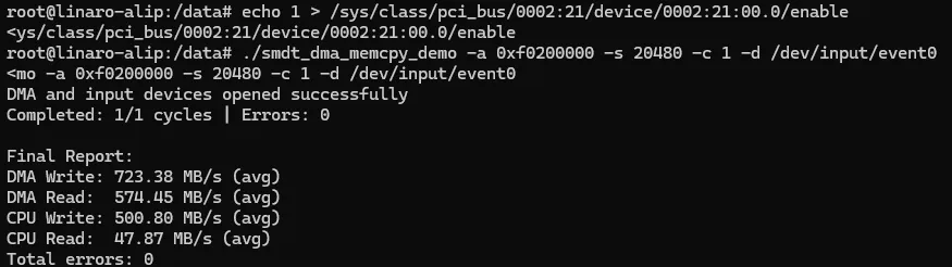
Info
If there is no error in either read or write, the DMA interaction is normal. -a indicates the address -s indicates the number of bytes transferred -c indicates the number of transfers -d indicates the device path You can adjust s and c to change the amount of data transferred by DMA.
4.3 Source Code Analysis
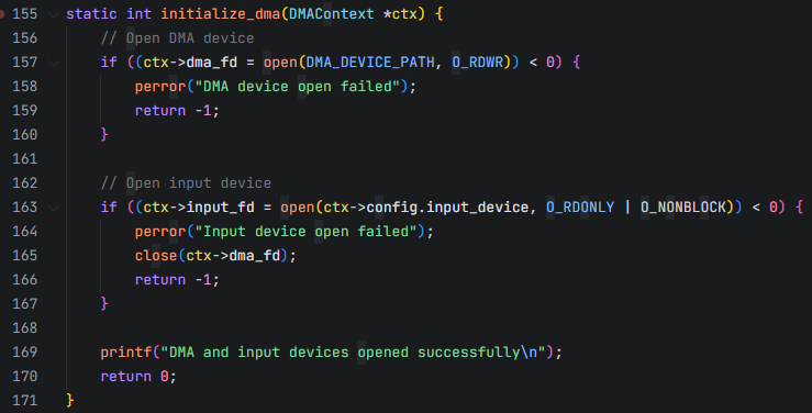
1️⃣ Open the device node
2️⃣ Write Test Phase Code Analysis (ARM -> FPGA)
Info
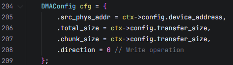
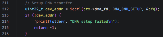
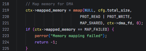
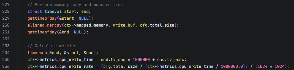
Function: static int perform_write_test(DMAContext *ctx, uint16_t *write_buf); Flow: ARM prepares data → DMA configuration → memory mapping → CPU copy → DMA transfer → wait for completion
- DMA configuration
- Establish DMA channel
- Establish memory mapping
- CPU data copy and performance test
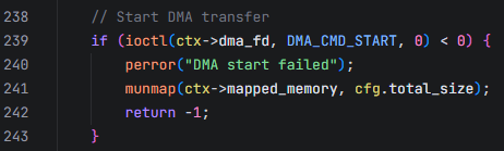
Start DMA
Start DMA via the
ioctlfunction to transfer data to the FPGA DRAM over the PCIe bus.
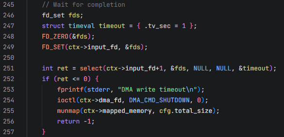
Wait for transfer completion
The program waits to receive the input event reported by the driver.
Get DMA transfer performance metrics
After the program receives the input event reported by the driver, it means the DMA transfer is complete. It gets the time consumed by the DMA data transfer via the
ioctlfunction and calculates the DMA transfer rate.

Cleanup and close
- Clean up the memory mapping
- Close the DMA transfer and return the status

3️⃣ Read Test Phase Code Analysis (FPGA -> ARM)
Info
Function: static int perform_read_test(DMAContext *ctx, uint16_t *write_buf, uint16_t *read_buf); Flow: DMA configuration → DMA transfer start → wait for completion → memory mapping → CPU copy → data verification
- DMA configuration
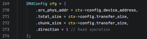
- Establish DMA channel
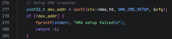
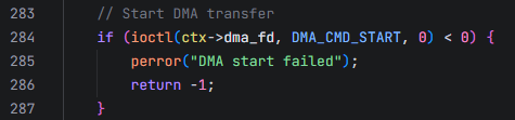
Start DMA
Start DMA via the
ioctlfunction to transfer FPGA DRAM data to the contiguous memory space allocated by the driver (located in DDR) over the PCIe bus.
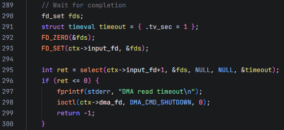
- Wait for FPGA data transfer
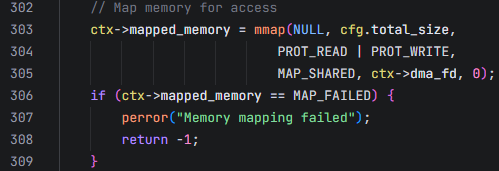
- Establish memory mapping
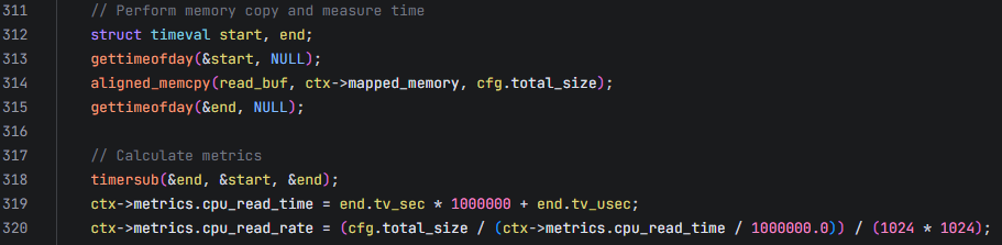
Read data
After the program receives the input event reported by the driver, it reads the data from kernel space to user space.
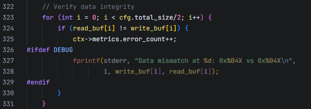
Data integrity verification
Verify whether the data is consistent with the written data.
Get DMA performance metrics
Get the time consumed by the DMA data transfer via the
ioctlfunction and calculate the DMA transfer rate.

Cleanup and close
- Clean up the memory mapping
- Close the DMA transfer and return the status

4.4 ioctl Function
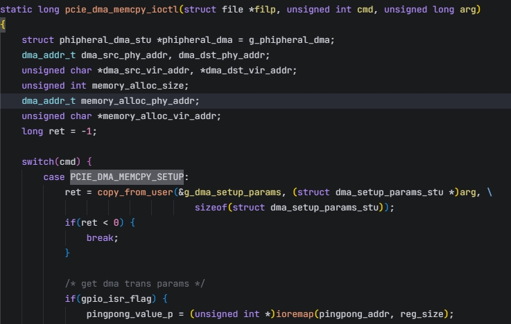
For the specific implementation, see the smdt_pcie_dma_memcpy.c file in the kernel source code. Some of the code is as follows:
Specific file path
File path: SDK/kernel-6.1/drivers/pci/pcie/smdt_pcie_dma_memcpy.c
4.5 FPGA Section Details
For FPGA-related content in PCIe communication testing, please refer to: PCIe-Based DMA/PIO Control Experiment