
FPGA Development Manual
1 Using and Adding Pango IP Cores
1.1 Experiment Introduction
Experiment purpose: Understand how to install IPs in the PDS software, use IPs, and view IP manuals.
Experiment environment: Window11 PDS2022.2-SP6.4 Chip model: PG2L50H-484
1.2 Experiment Principle
1.2.1 IP Installation
After the PDS software is installed, PDS comes with some basic IPs. Other IPs require the user to download the IP installation package and install the IP.
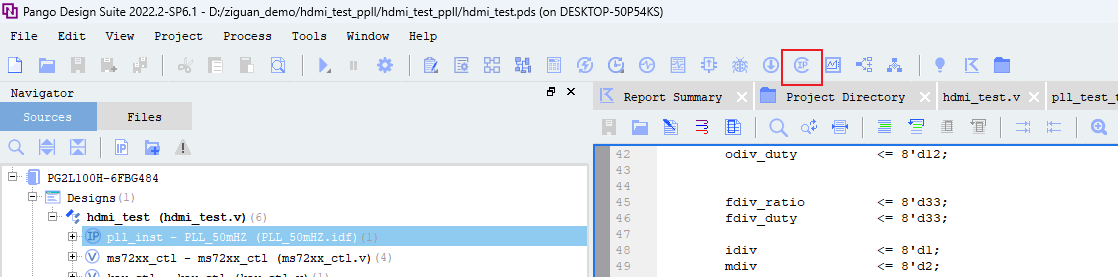
After opening PDS, click the IP icon in the red box above.
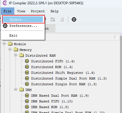
Then in the pop-up tab, click File->Update... in the upper-left corner.
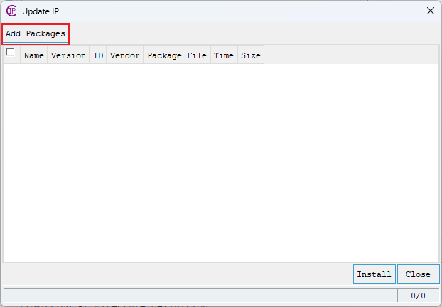
Click Add Package in the upper-left corner.
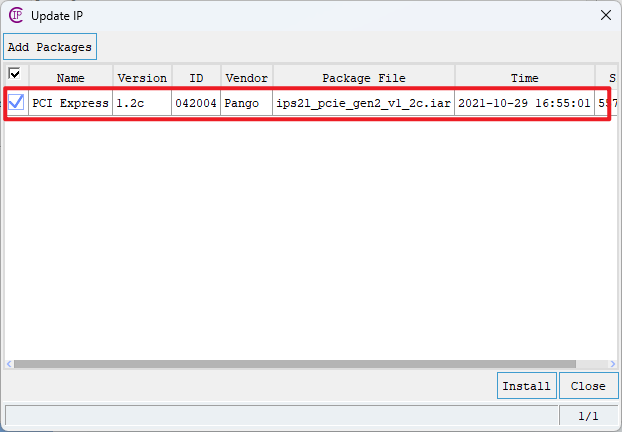
The figure above shows the installation files of the PCIE IP, with the suffix .iar. After selecting the corresponding file, click Open in the lower-right corner. Then tick the front √, and click Install.
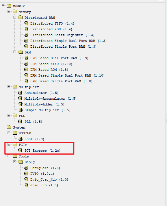
Then you can see the IP just installed in the left panel. Note that if a warning pops up after installation and the left panel does not change, it means the IP you installed is not supported by this series of devices. Because your project might be LOGOS, LOGOS2, or Tian2 series, and the IPs used by different chip models are slightly different, so please pay attention to this point.
1.2.2 Instantiating an IP and Viewing the IP Manual
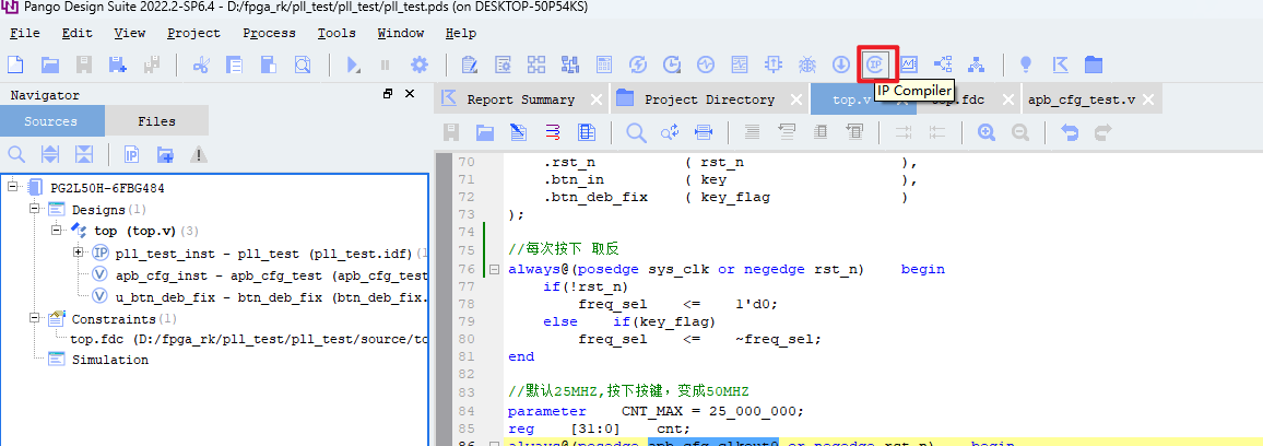
Continue to click the icon in the red box above.
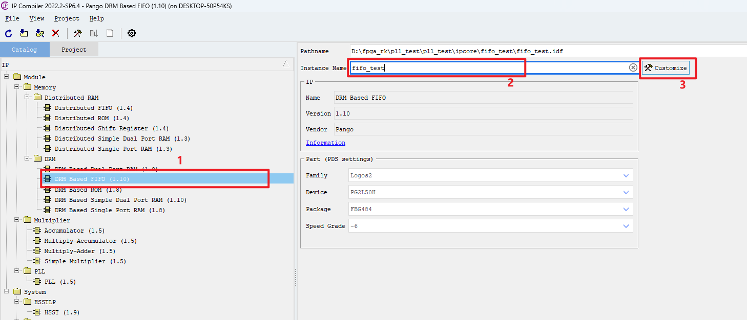
Select the IP you want to generate. Here we take FIFO as an example, as shown in red box 1. Red box 2 is used to fill in the name of the generated IP. Click red box 3 to generate the IP and pop up the configuration interface for this IP, as shown in the figure below:
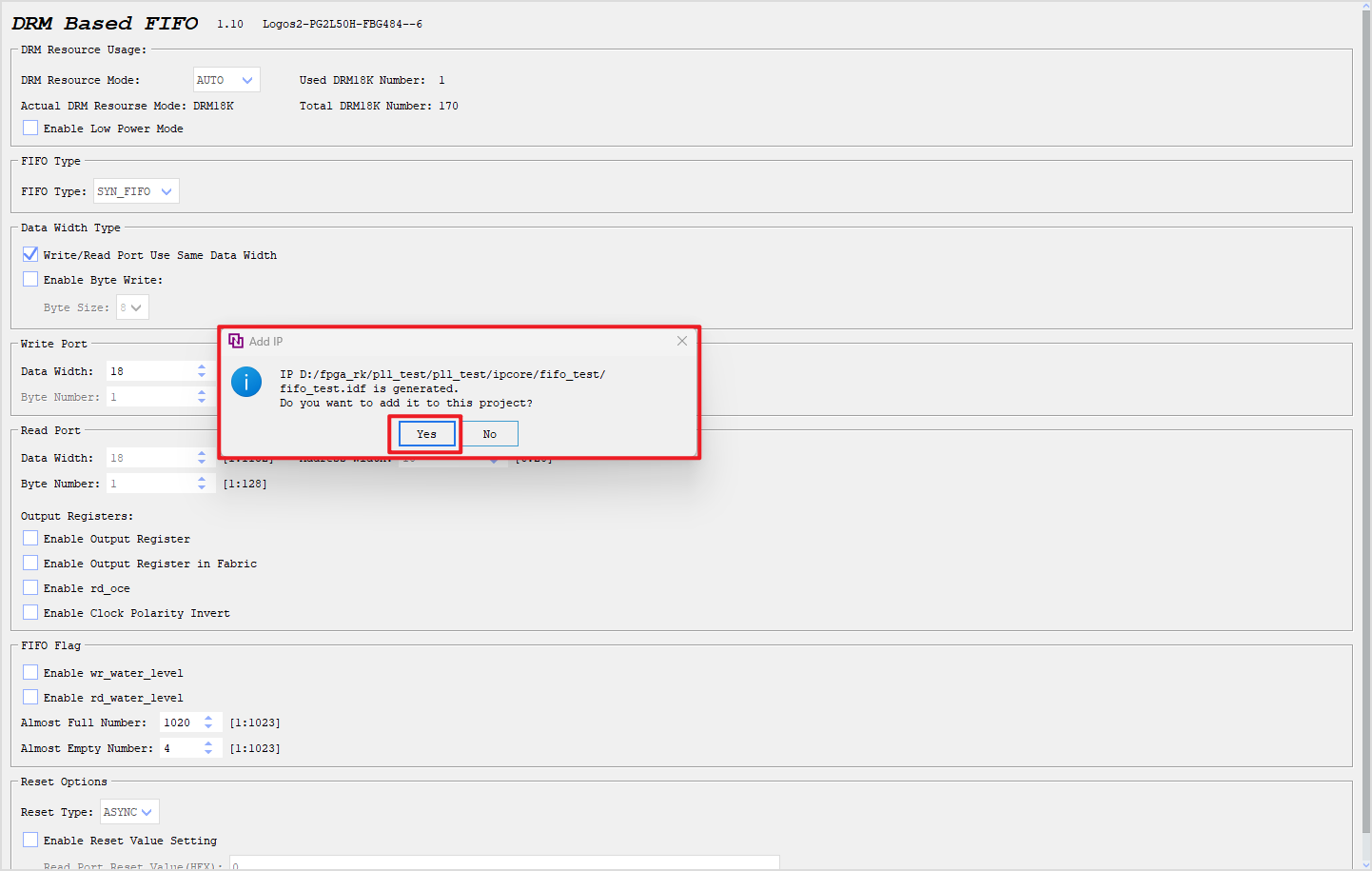
The pop-up prompt asks whether we want to add the IP to the project. Just click YES. If we don't know how to use the IP, we can open the official reference manual to view it, as shown in the figure below:
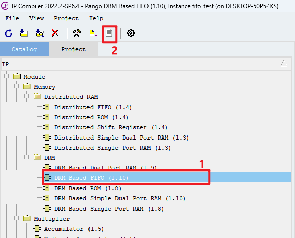
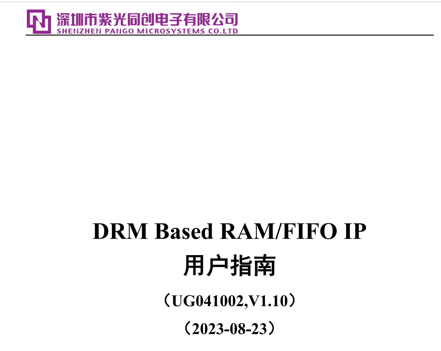
Select the IP you want to view, then click the icon shown in red box 1 to automatically pop up the official reference document.
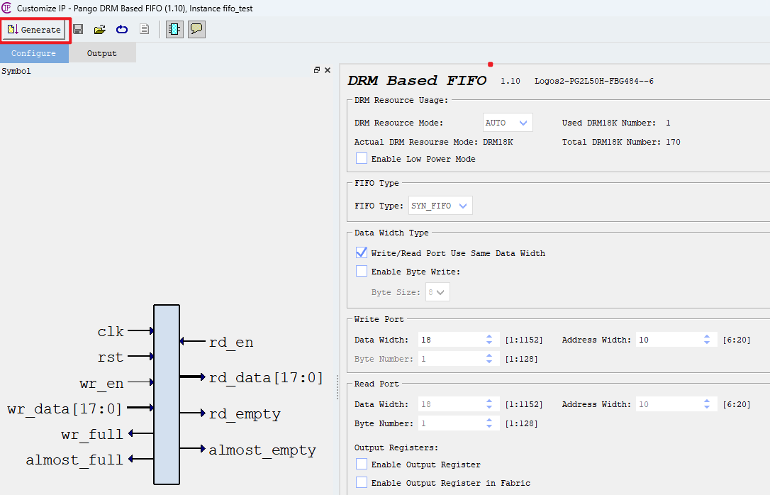
After configuring the IP, click Generate at red box 1 in the upper-left corner.
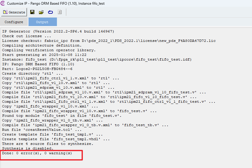
No errors means generation succeeded.
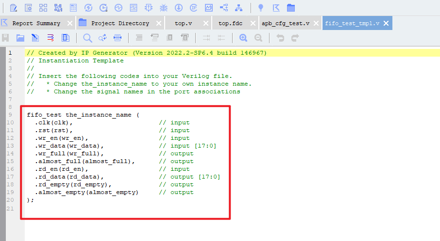
At the same time, the tool will automatically pop up an instantiation template of the IP for us to use. Just add this instantiation template to your own project to use the generated IP.
2 Key-Controlled LED Experiment
2.1 Experiment Introduction
Experiment purpose: From creating a project to writing code, completing pin constraints, and finally generating a bitstream and downloading it to the development board, complete Key0 controlling led0 blinking and Key1 controlling led1 on/off. Experiment environment: Window11 PDS2022.2-SP6.4 Chip model: PG2L50H-484
2.2 Experiment Principle
The carry-over of the usual hour, minute, and second timing should be familiar to everyone;
1 hour = 60 minutes = 3600 seconds. When the hour hand rotates 1 hour, the second hand beats 3600 times;
The clock signal in a digital circuit also has a fixed rhythm. The time from the start to the end of this rhythm is usually called the period (T).

In a digital system, we usually pay attention to the clock frequency. The relationship between frequency and period is as follows:
f=1/T
The crystal oscillator on this development board provides a 25MHz single-ended clock.
So its period is about 40ns. In our FPGA design, our always block usually assigns data at the rising edge of the clock, so we can define a variable. Every time the clock rising edge arrives, the variable is incremented by 1, turning it into a counter. Each increment of 1 means 40ns has passed. So to time 1s, just let it count to 24999999, because counting starts from 0, so counting to 24999999 is exactly one second. By analogy, 12499999 is 0.5s.
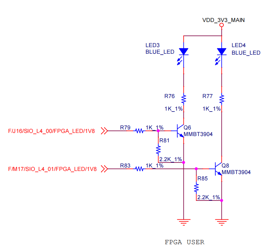
The figure above is the schematic of the 2 LED lights on the development board.
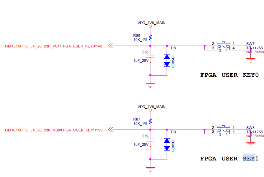
The figure above is the schematic of the 2 buttons on the development board.
KEY0 controls LED0 to change its state every 1s, and KEY1 controls the on/off state of LED1. (High level is represented by 1, low level by 0)
2.3 Interface List
top.v top-level module interface list:
| Port | I/O | Width | Description |
|---|---|---|---|
| sys_clk | input | 1 | System clock 25MHz |
| key0 | input | 1 | User button 0 |
| key1 | input | 1 | User button 1 |
| led_0 | output | 1 | LED control signal |
| led_1 | output | 1 | LED control signal |
btn_deb_fix.v button debouncing module interface list:
| Port | I/O | Width | Description |
|---|---|---|---|
| BTN_WIDTH | parameter | 4 | Number of buttons |
| sys_clk | input | 1 | System clock 25MHz |
| rst_n | input | 1 | Global reset |
| btn_in | input | BTN_WIDTH | User button input |
| btn_deb_fix | output | BTN_WIDTH | Debounced button output (pulse signal) |
2.4 Project Description
The project framework is as follows:
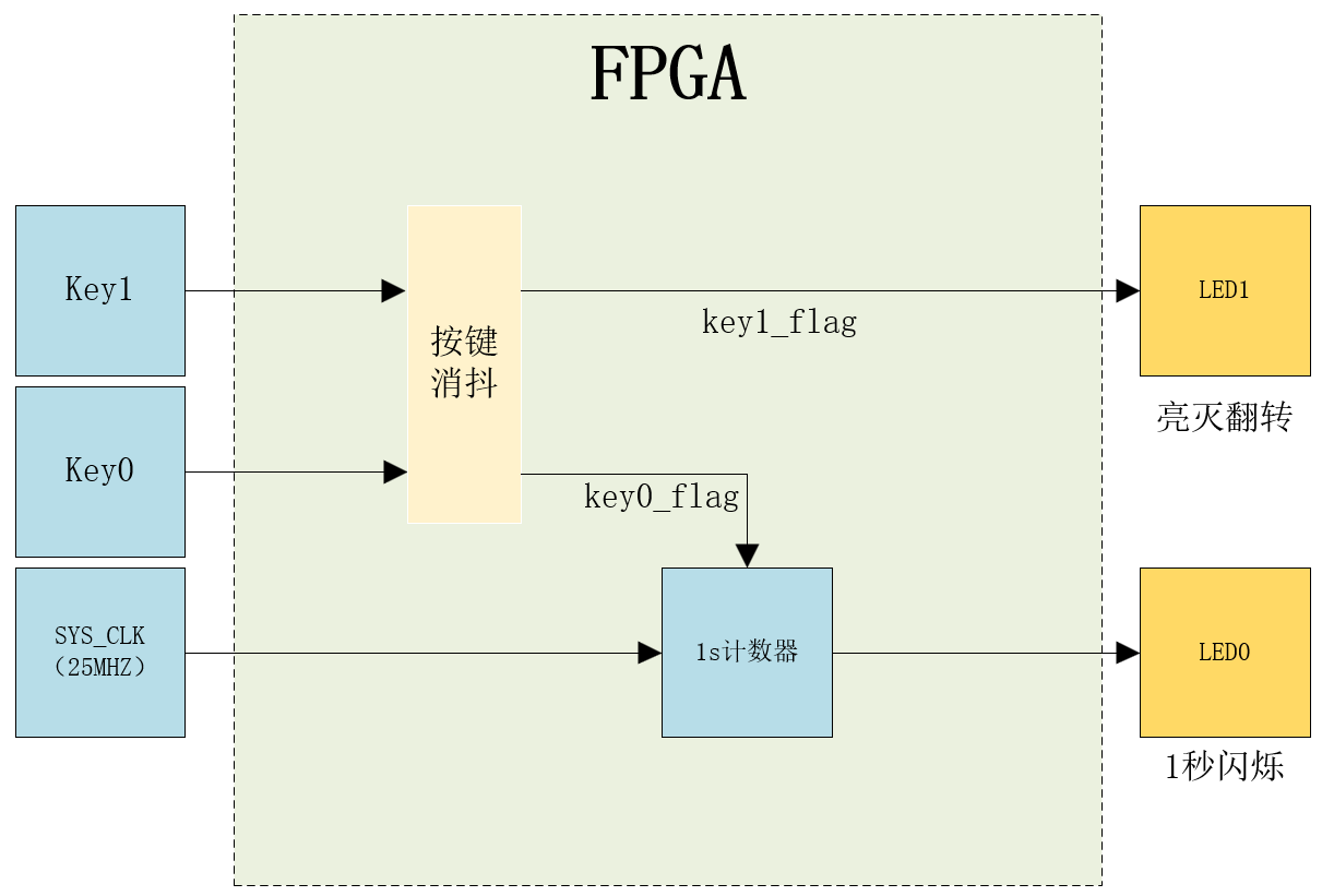
This project mainly completes button-controlled LED states. Button 0 controls led0 blinking, and button 1 controls led1 on/off.
First, key0 and key1 both go through the button debouncing module, because the development board uses mechanical buttons, so every press will produce jitter. If not debounced, it will cause misjudgment. After debouncing, each button press produces a high level lasting one clk, i.e., key0_flag and key1_flag. key0_flag controls whether to enable the 1s counter to start led0 blinking. key1_flag directly controls LED1 toggling — each press of key1 toggles the led state once.
2.5 Code Module Description
//key0->led0	闪烁
//key1->key1	翻转
module	top(
input	wire	sys_clk	","	//系统时钟25MHZ
input	wire	key0	","
input	wire	key1	","

output	reg	led_0	","
output	reg	led_1
);
//----------------------------------parameter----------------------------------------
parameter	CNT_MAX	=	32'd25_000_000	;	//1s计数

//----------------------------------reg----------------------------------------------
reg	[7:0]	rsn_cnt	0	;	//复位计数器
reg	[31:0]	cnt_1s	;	//计数器
reg	led0_en	;	//led0闪烁使能

//----------------------------------wire----------------------------------------------
wire	rst_n	;	"//复位信号,低电平有效"
wire	key0_flag	;	//按键按下后的上升沿
wire	key1_flag	;	//按键按下后的上升沿

//----------------------------------always	&	assign----------------------------------------------
//产生复位
always@(posedge	sys_clk)	begin
if(rsn_cnt	>=100)
rsn_cnt	<=	rsn_cnt;
else
rsn_cnt	<=	rsn_cnt	+	1'b1;
end
assign	rst_n	=	(rsn_cnt>=100)?1'b1:1'b0	;

//每按下一次key0进行一次翻转
always@(posedge	sys_clk)	begin
if(!rst_n)
led0_en	<=	1'd0;
else	if(key0_flag)
led0_en	<=	~led0_en;
end

//计数1s
always@(posedge	sys_clk)	begin
if(!rst_n)
cnt_1s	<=	32'd0;
else	if(led0_en)	//led0闪烁使能
begin
if(cnt_1s	==	CNT_MAX-1)	//1秒
cnt_1s	<=	32'd0;
else
cnt_1s	<=	cnt_1s	+	1'b1;
end
else
cnt_1s	<=	32'd0;
end

//led0	1s闪烁
always@(posedge	sys_clk)	begin
if(!rst_n)
led_0	<=	1'd0;
else	if(led0_en)
begin
if(cnt_1s	==	CNT_MAX-1)	//1s翻转led
led_0	<=	~led_0;
else
led_0	<=	led_0;
end
else
led_0	<=	1'd0;
end

//led1翻转
always@(posedge	sys_clk)	begin
if(!rst_n)
led_1	<=	1'd0;
else	if(key1_flag)
led_1	<=	~led_1;
end

//----------------------------------instance----------------------------------------------
//按键消抖模块
btn_deb_fix#(
BTN_WIDTH	(	4'd2	)	//2个按键
)u_btn_deb_fix(
sys_clk	(	sys_clk	"),"
rst_n	(	rst_n	"),"
btn_in	(	"{key1,key0}"	"),"
btn_deb_fix	(	"{key1_flag,key0_flag}"	)
);


endmodule
CNT_MAX defines a maximum count value. Since our system clock is 25MHz, which is 25000000, to make the LED blink every 1s, we count from 0 to 24999999 and toggle the led.
In lines 26-31, a reset signal is generated after counting 100 cycles of the system clock, providing reset for subsequent modules and sequential logic.
In lines 43-55, the one-second counting starts only when led0_en is pulled high. Otherwise, the counter always stays at 0.
In lines 82-89, a button debouncing module is instantiated. After a button is pressed and released, a pulse signal is generated, namely key0_flag and key1_flag. key0_flag controls led0 blinking, and key1_flag controls led1 toggling.
//按键消抖
`define	UD	#1
module	btn_deb_fix#(
parameter	BTN_WIDTH	=	4'd8	//按键数量
)
(
input	sys_clk	","
input	wire	rst_n	","
input	[BTN_WIDTH-1:0]	btn_in	","

output	reg	[BTN_WIDTH-1:0]	btn_deb_fix
);

//----------------------------------parameter----------------------------------------
parameter	CNT_20MS_MAX	=	32'd500_000	;	//20MS计数

//----------------------------------reg----------------------------------------------
reg	[23:0]	cnt[BTN_WIDTH-1:0];	//计数器
reg	[BTN_WIDTH-1:0]	btn_in_reg	;	//寄存按键信号
//打一拍
always	@(posedge	sys_clk)	begin
btn_in_reg	<=	btn_in;
end
//----------------------------------消抖主要逻辑----------------------------------------------
genvar	i;
generate
begin
for(i=0;i<BTN_WIDTH;i=i+1)
begin
always	@(posedge	sys_clk)	begin
if(!rst_n)
cnt[i]	<=	24'd0;
if	(btn_in_reg[i]	==	1'b0)	//按下时	计数20ms时归零
cnt[i]	<=	24'd0;
else	if(cnt[i]==CNT_20MS_MAX)	//抖动区间有效时计数
cnt[i]	<=	cnt[i];
else
cnt[i]	<=	cnt[i]	+	1'b1;
end

always	@(posedge	sys_clk)	begin
if(!rst_n)
btn_deb_fix[i]	<=	1'd0;
else	if(cnt[i]==CNT_20MS_MAX-1)	//消抖后输出一个clk的高电平
btn_deb_fix[i]	<=	1'b1;
else
btn_deb_fix[i]	<=	1'b0;
end
end
end
endgenerate

endmodule
This part is the button debouncing module. parameter defines the number of button inputs. The output of the module produces a pulse signal, i.e., a high-level signal lasting one clk.
In lines 30-50, cnt continuously counts 20ms. When a button is pressed, cnt resets to 0 and starts counting from 0 up to 20ms. When it counts to 20ms, it outputs a high level for one clk, i.e., sets btn_deb_fix to 1 and keeps it for only one clk.
2.6 Experiment Steps
Here we describe in detail the specific steps from creating a new project to downloading the program. Subsequent projects will not be explained in such detail.
2.6.1 Open the PDS Software and Create a Project
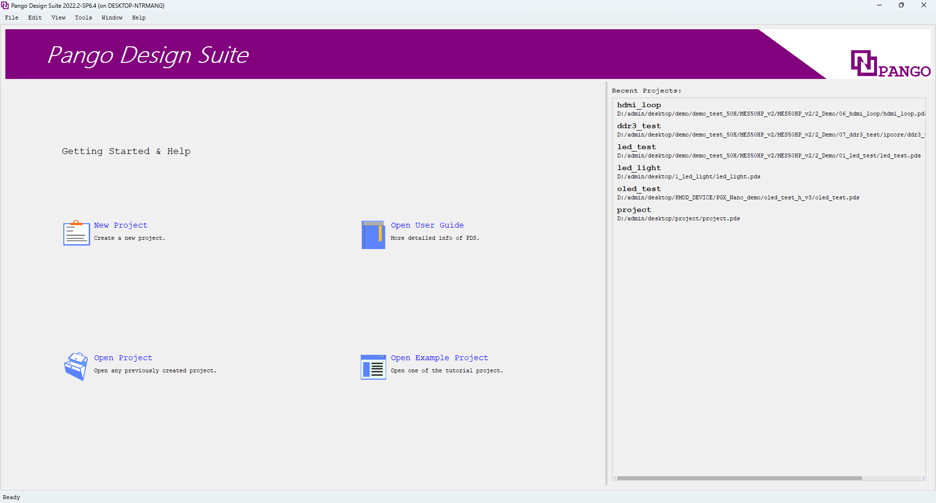
Step 1: Open the PDS software, click NEW Project, and then complete the new project setup.
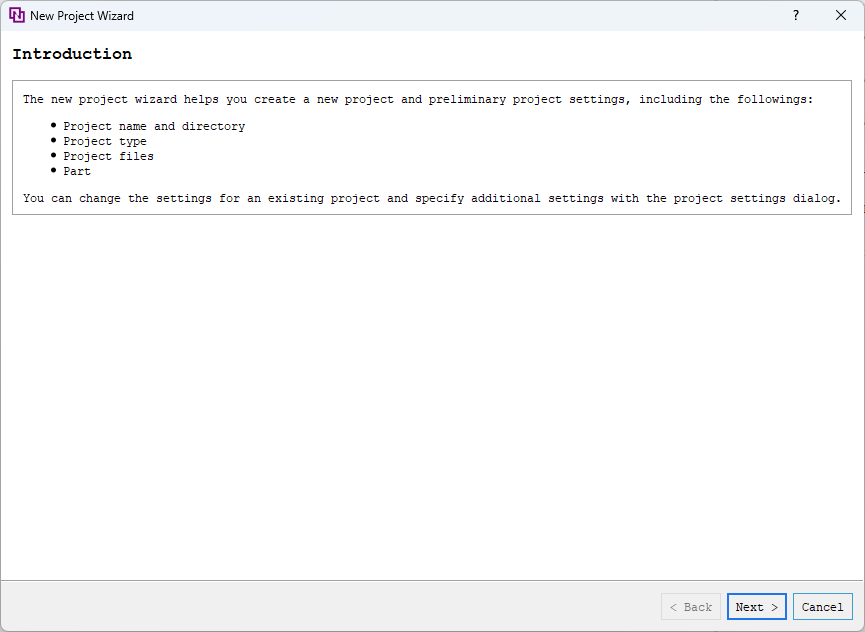
Step 2: Click NEXT
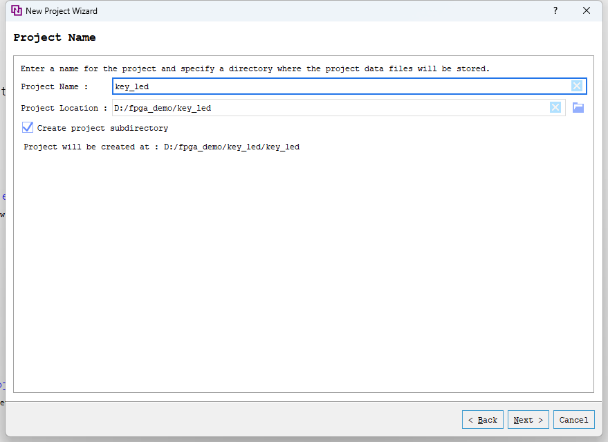
Step 3: Create a project named led_water in the corresponding directory, then click Next.
Creating a new project mainly includes setting the project name and path, project type, project files, and device information.
[Project Name] is the project file name, which defaults to project. (Only letters, digits, underscores (_), hyphens (-), and dots (.) are allowed).
[Project Location] is used to select the working path of the new project. Folder names allow only letters, digits, underscores (_), hyphens (-), dots (.), @, ~, comma, +, =, #, and space ( ), but spaces must not appear at the beginning or end of the path name. That is, the path where the project files are placed.
[Create Preject Subdirectory] makes the project file name part of the working directory.
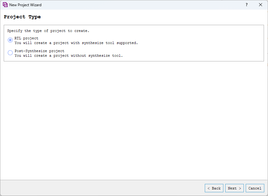
Step 4: Select RTL project and click Next.
[RTL Project] is used to create an RTL project. The new project can perform synthesize, device map, place& route, report timing, report power, generate netlist, and generate bitstream.
[Post-Synthesize Project] is used to create a post-synthesis project. The new project can perform device map, place& route, report timing, report power, generate netlist, and generate bitstream.
Step 5: Click Next
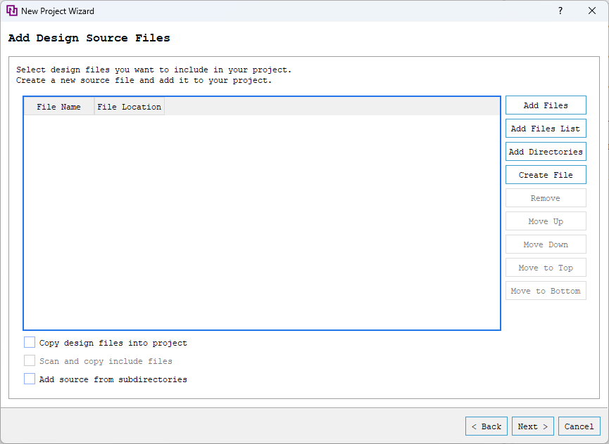
This interface allows you to use Add Files and Add Directories to add RTL source files and create new RTL source files, as well as adjust the compile order of RTL files. Add Files adds the selected files, and Add Directories adds all suitable files under the selected folder. If Add source from subdirecotires is checked below, suitable files in all subdirectories are added. You can also skip adding files directly by clicking NEXT.
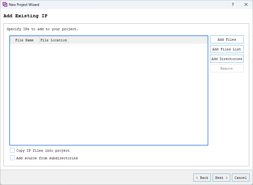
Step 6: Click Next
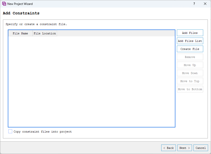
Step 7: Click Next
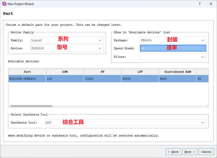
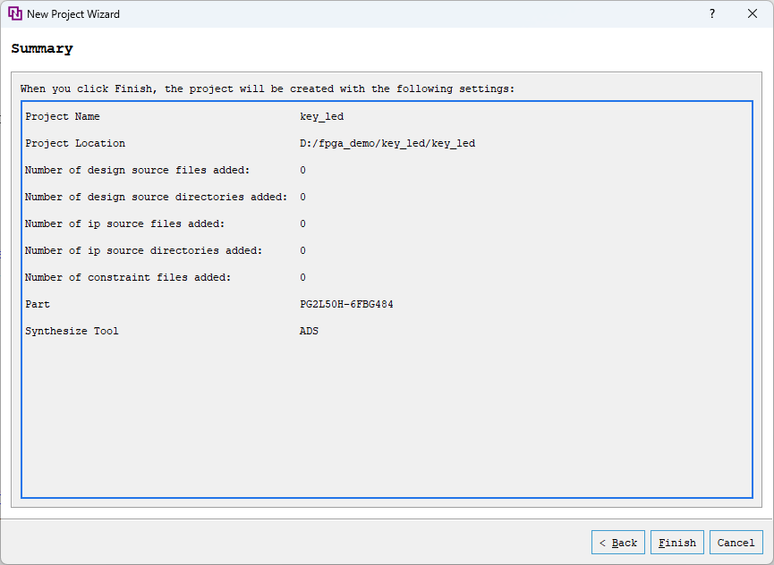
Step 8: Select the device family, model, package, speed, and synthesis tool, then click Next
In the synthesize tool, you can choose Synplify Pro or ADS as the synthesis tool. In this experiment, the ADS synthesis tool is used.
Step 9: Click Finish in summary to complete the project creation.
2.6.2 Add Design Files
The PDS software interface is shown below:
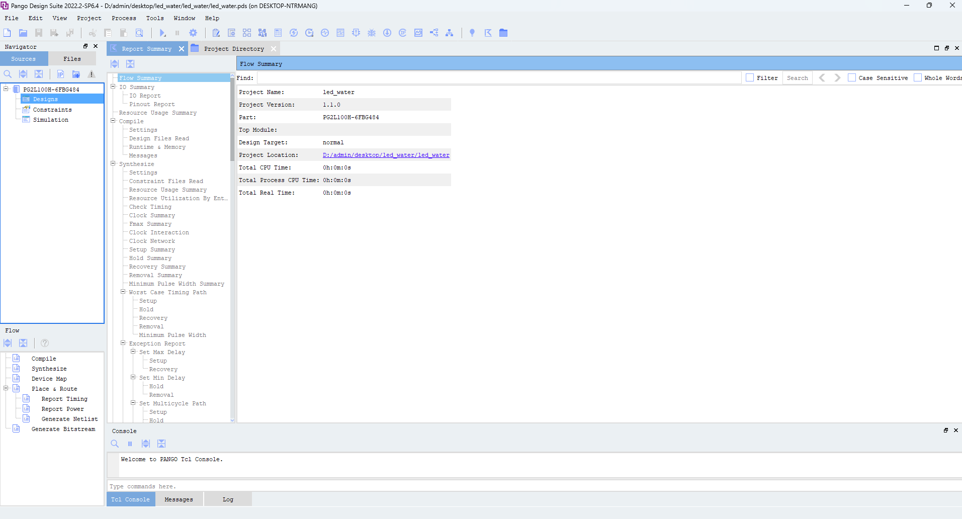
Double-click Designs, add the previously designed module to the file, or add the previously edited verilog file to the project:
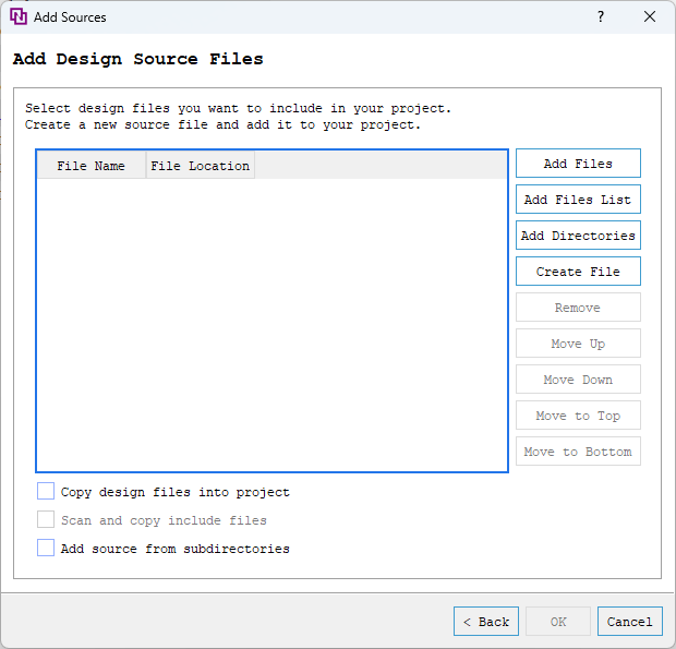
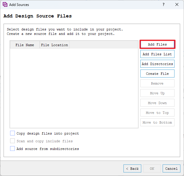
Add files to the project:
Click Add Files in the window to add files to the project;
Create a new file in the project:
- Click Create File in the window;
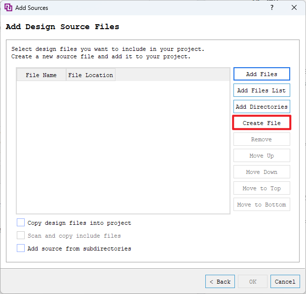
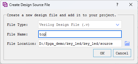
- Select Verilog Design File, the file name must match the module name, keep the default path, and click OK;
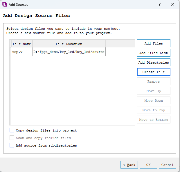
- Click OK;
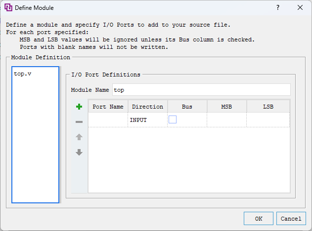
- Click Cancel;
- The newly created file is opened by default. Copy the previously designed code into it,
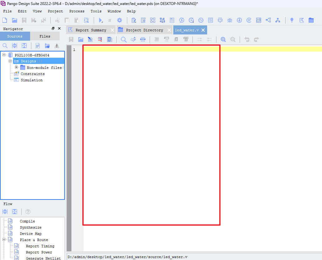
- Click save to complete creating the new file
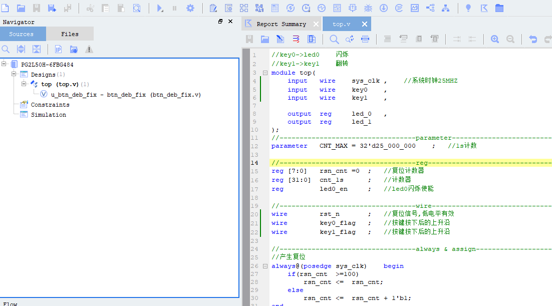
Press Ctrl+s to save.
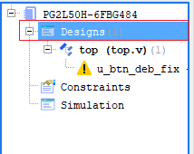
Double-click Designs.
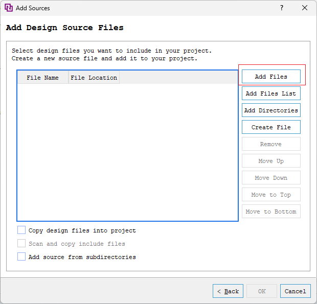
Click Add Files;
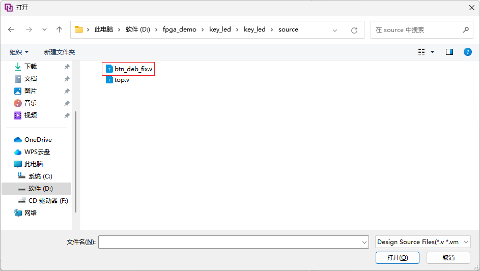
Add the btn_deb_fix.v module, i.e., the button debouncing module.
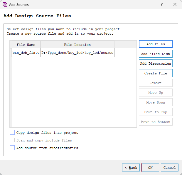
Click OK.
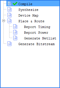
2.6.3 Compile
You can run the Compile flow in the following ways:
(1) Double-click Compile in Flow to run synthesis;
(2) Right-click Compile and click Run to run synthesis;
2.6.4 Project Constraints
Click Tools, select User Constraint Editor(Timing and Logic), or click the toolbar icon, User Constraint Editor(Timing and Logic), and select Pre Synthesize UCE, as shown below.
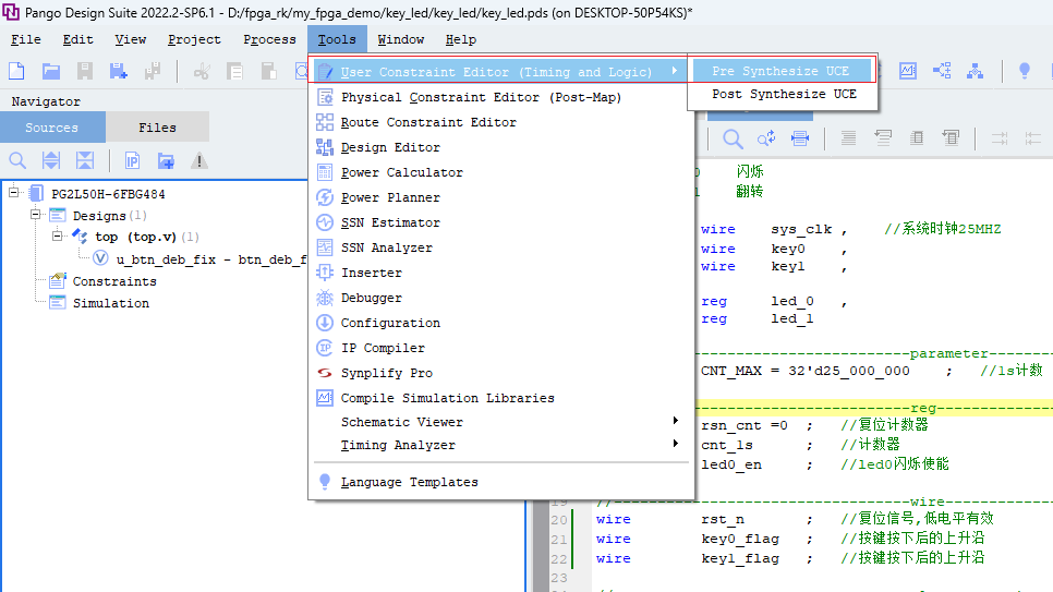
User Constraint Editor(Timing and Logic) under Tools
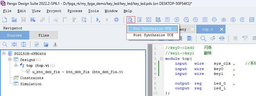
User Constraint Editor(Timing and Logic) icon on the toolbar
2.6.4.1 Clock Constraints
After opening the UCE, select Timing Constraints, then select Create Clock to add the reference clock. The reference clock is usually the on-board clock input by the user through an input port.
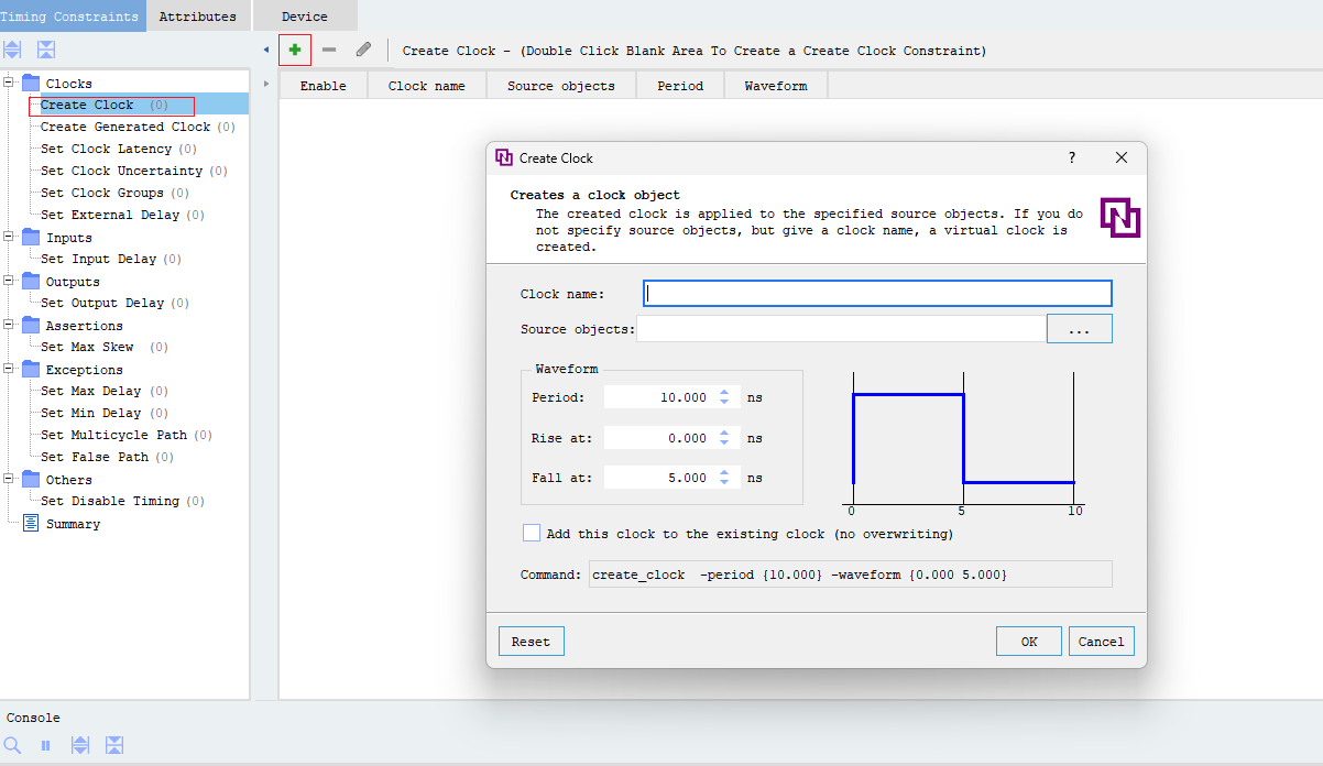
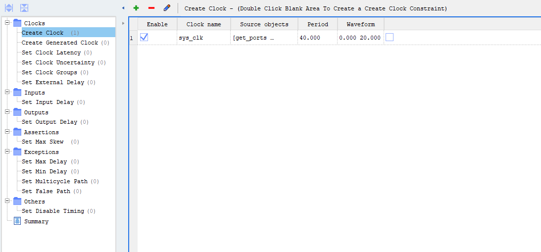
In the popup, name the clock, associate the clock pin, and add the clock parameters. Clicking OK creates a clock constraint; Reset resets this page. After creation, it looks like the figure below:
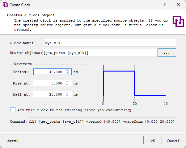
The clock provided to the development board is 25MHz, i.e., a period of 40ns.
2.6.4.2 Physical Constraints
After opening the UCE, select Device, then select I/O, and edit the IO assignment according to the schematic.
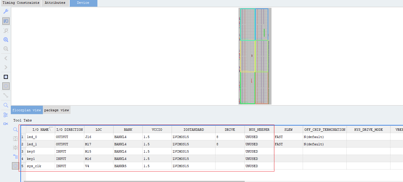
After editing the IO assignment according to the schematic, click save to generate a .fdc file and complete the constraints.
2.6.5 Synthesize
There are four ways to run the Synthesize flow:
(1) Double-click Synthesize in Flow to run synthesis;
(2) Right-click Synthesize and click Run to run synthesis;
After completing the Synthesize operation, you will see the following:
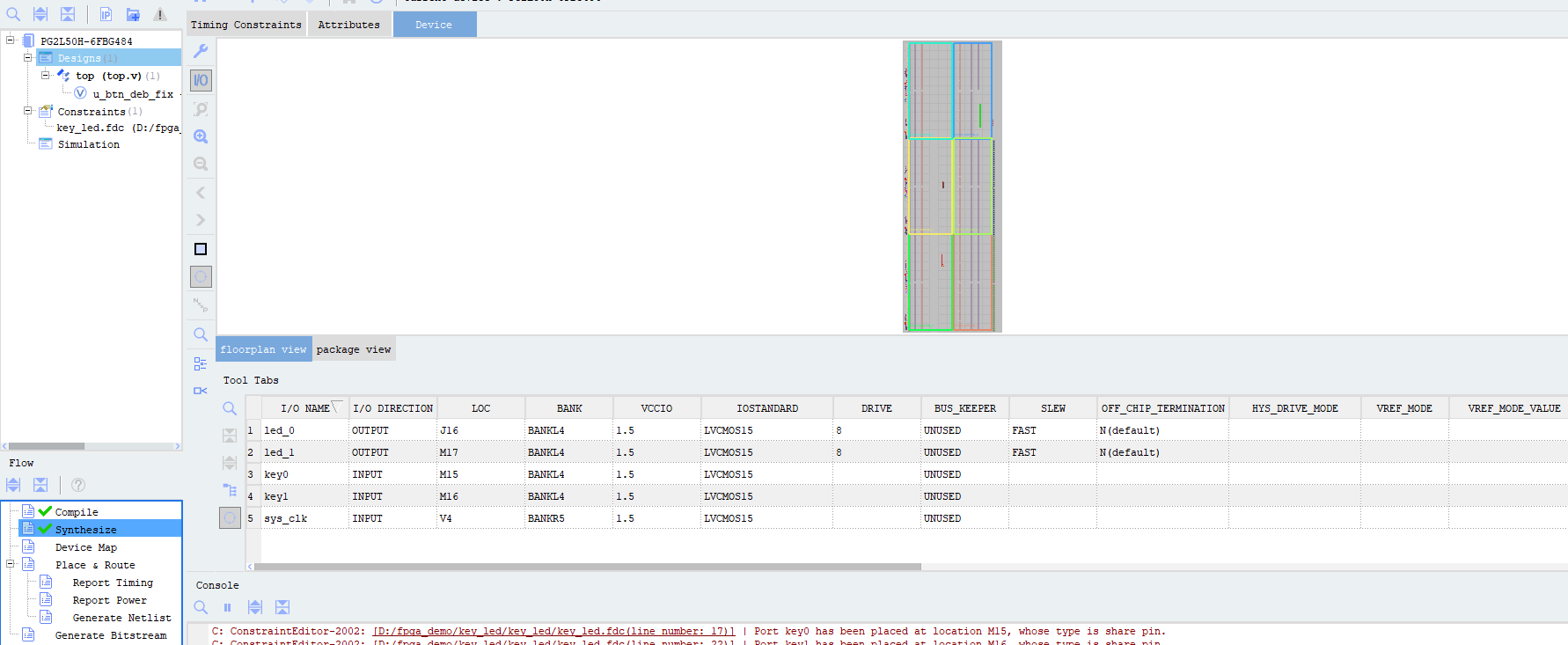
2.6.6 Device Map
The main purpose of Device Map is to map the design to the specific sub-units of the model (LUT, FF, Carry, etc.). The Device Map flow can be run in the following ways:
(1) Double-click Device Map directly;
(2) Right-click Device Map and click Run;
After completing the Device Map operation, you will see the following:
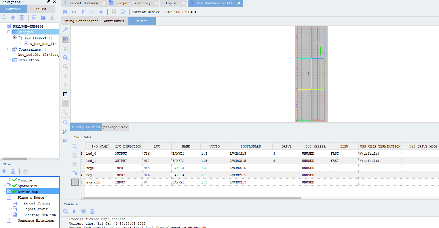
2.6.7 Place & Route
Place & Route performs actual placement and routing of design modules according to user constraints and physical constraints. The Place & Route flow can be run in the following ways:
(1) Double-click Place & Route directly;
(2) Right-click Place & Route and click Run;
After completing the Device Map operation, you will see the following:
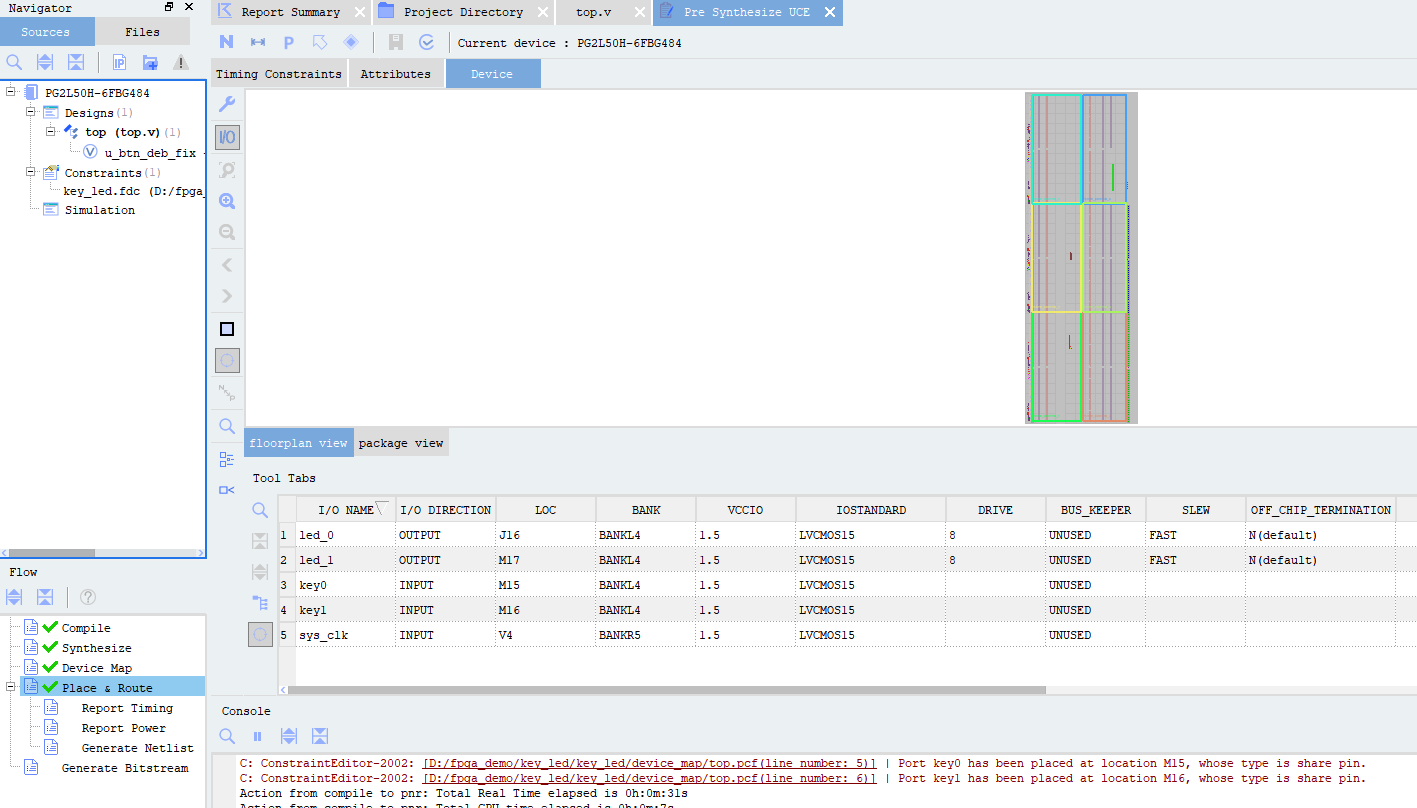
2.6.8 Generate Bitstream
Generate Bitstream generates a binary bitstream file. The Generate Bitstream flow can be run in the following ways:
(1) Double-click Generate Bitstream directly;
(2) Right-click Generate Bitstream and click Run;
After completing the above operations, a bitstream file will be produced. Running Generate Bitstream, you can see the interface as shown below:
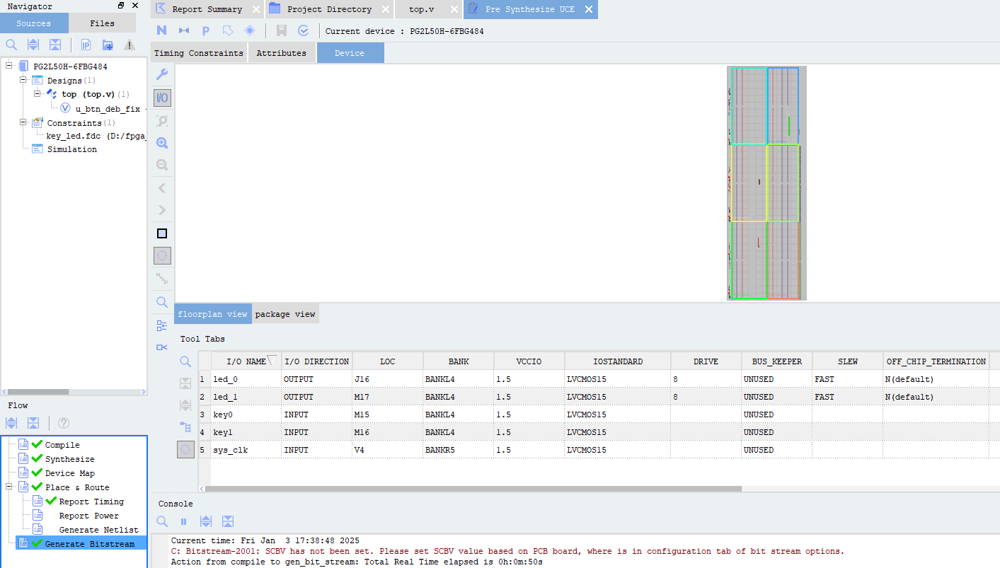
2.6.9 Download the Generated Bitstream File
Click Tools, select Configuration, or click the Configuration icon on the toolbar, as shown below.
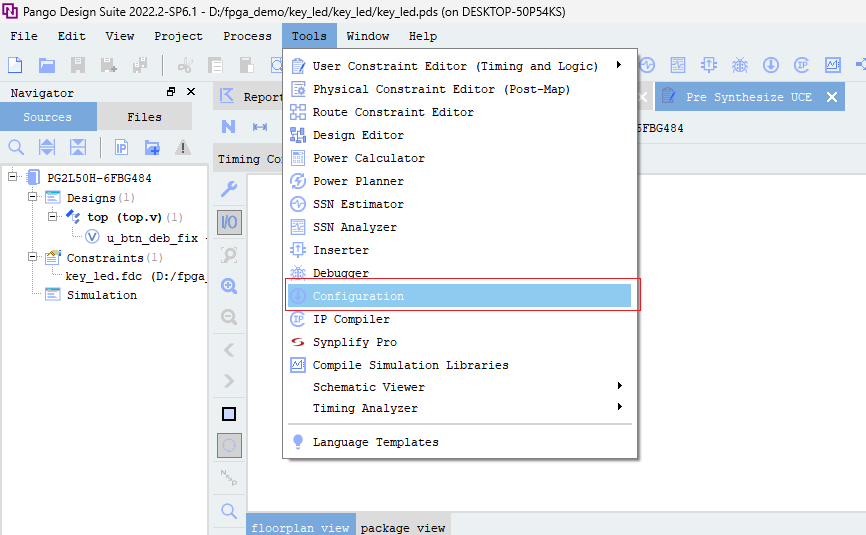
Configuration under Tools
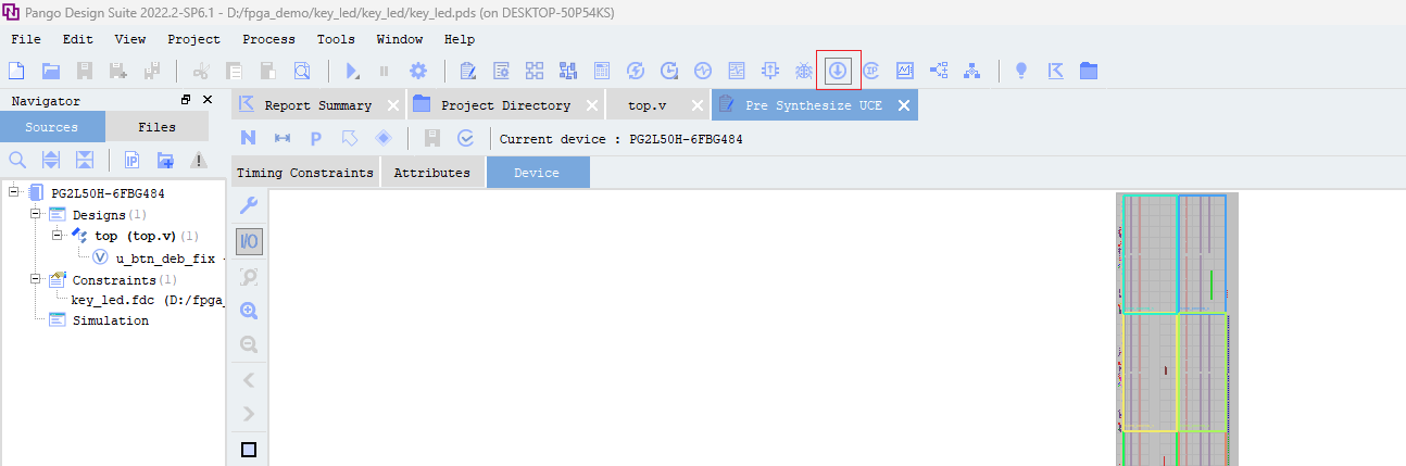
Configuration icon on the toolbar
After opening Configuration, directly select Scan Device to scan the Jtag chain. After the chain is initialized successfully, all devices scanned on the chain are displayed in the work area, and the device information of the current device is displayed in the device attribute window. A dialog box pops up showing the configuration files that can be added for the device:
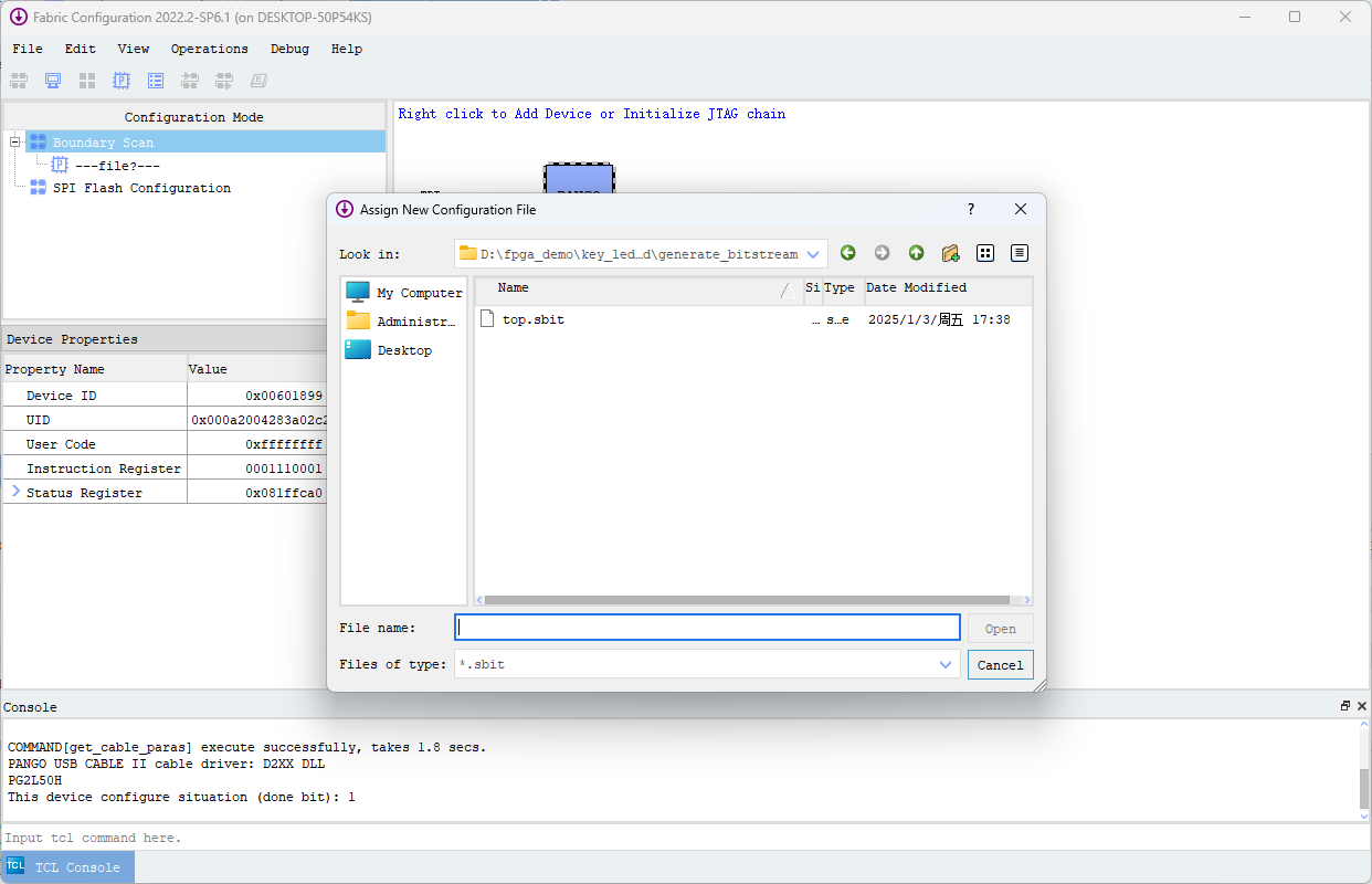
Chain initialized successfully
In the dialog box, select the bitstream file, add this configuration file, prompt the absolute path of the loaded file and display it in the information bar, as shown below:
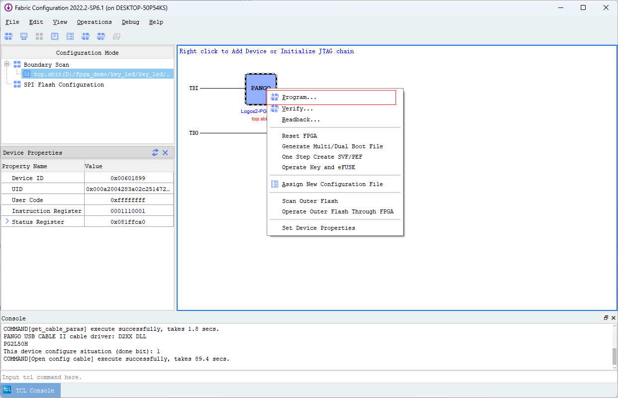
Download the bitstream file
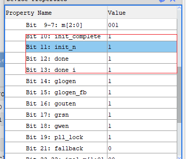
When all these 4 signals are 1, it means the download was successful.
At the same time, the development board is also equipped with an external flash. If you need to flash the program onto the board, you need to convert the bitstream file into an .sfc file.
First, click the Covert File option under the Operations option on the Configuration page.
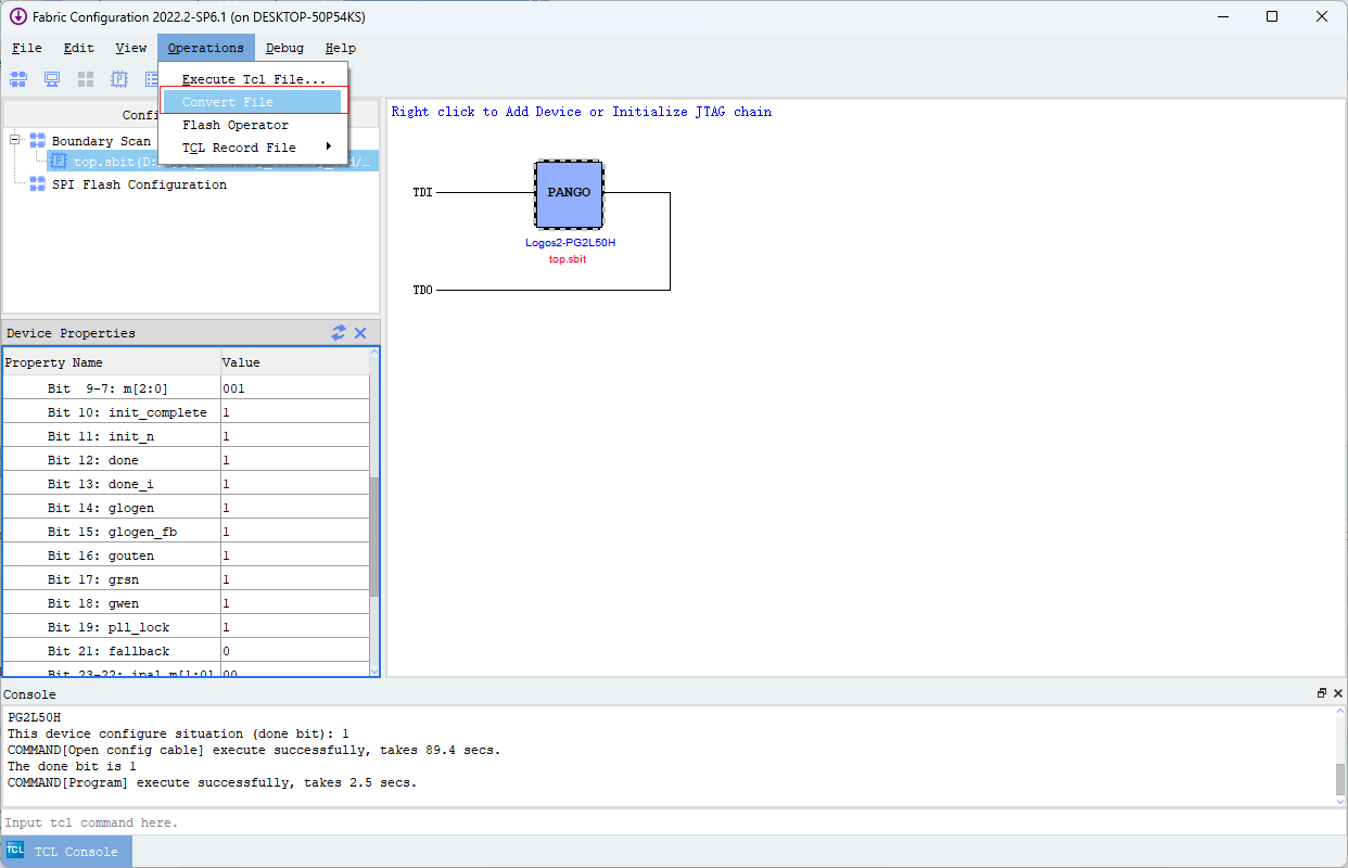
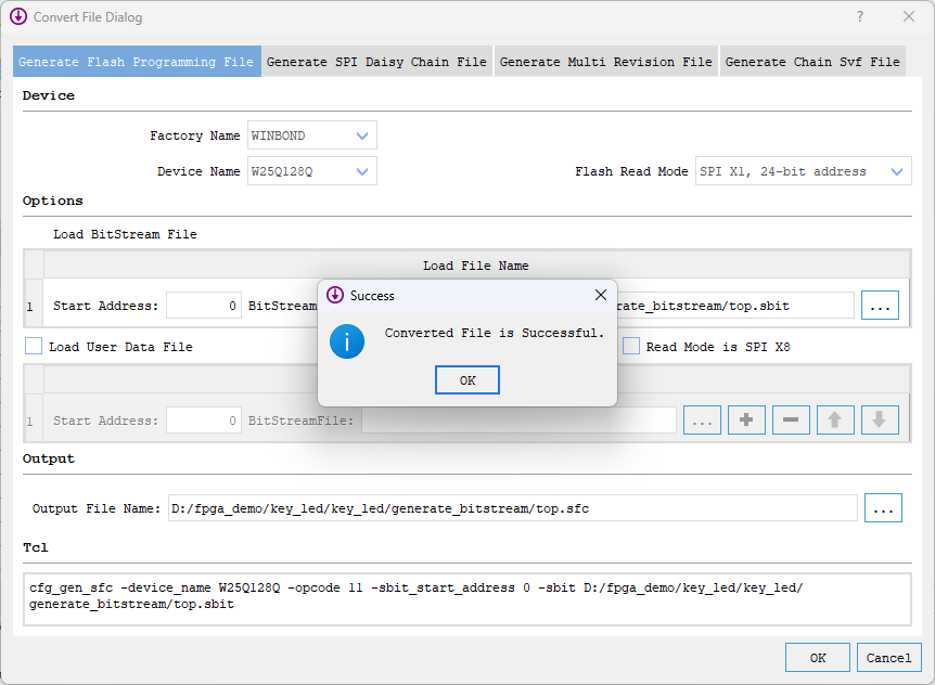
After clicking, the following screen appears. On the Generate Flash Programing File page, select the corresponding Flash device's manufacturer name and model, then select the path of the bitstream file at BitStreamFile, and click OK. (If the flash device you use is not in the optional flash list, you need to manually add the corresponding flash model. For the steps, please refer to the development board download and flashing instructions.)
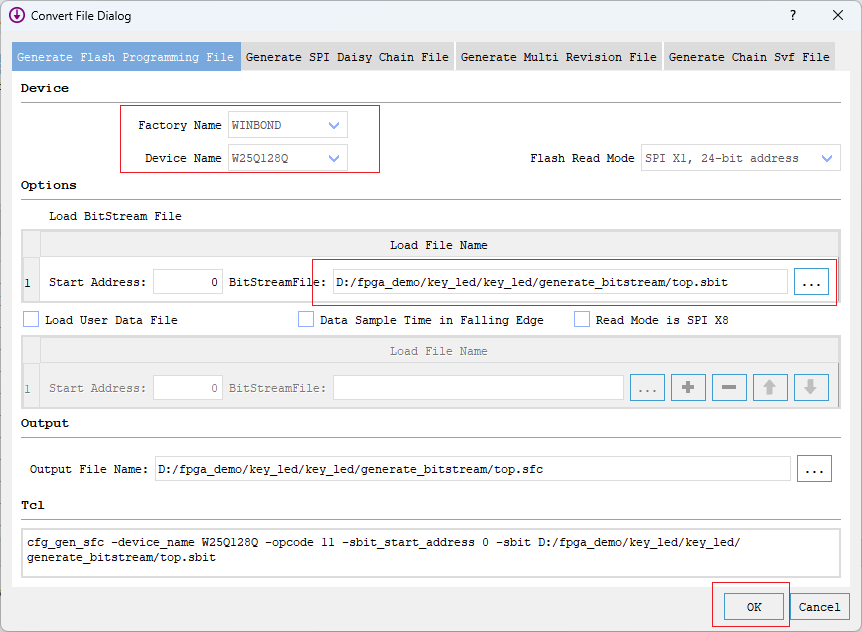
After the .sfc file is successfully converted, the page will look like the following. Click OK.
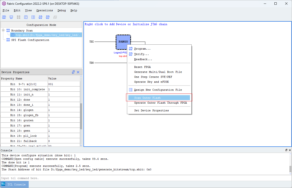
Users can right-click the position shown below and click Scan Outer Flash.
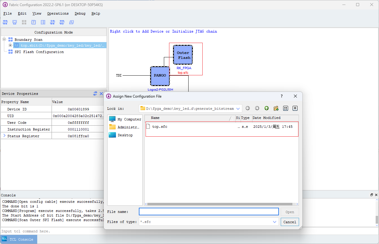
The page will display the model of the Flash mounted on the board. Click the .sfc file and click OPEN.
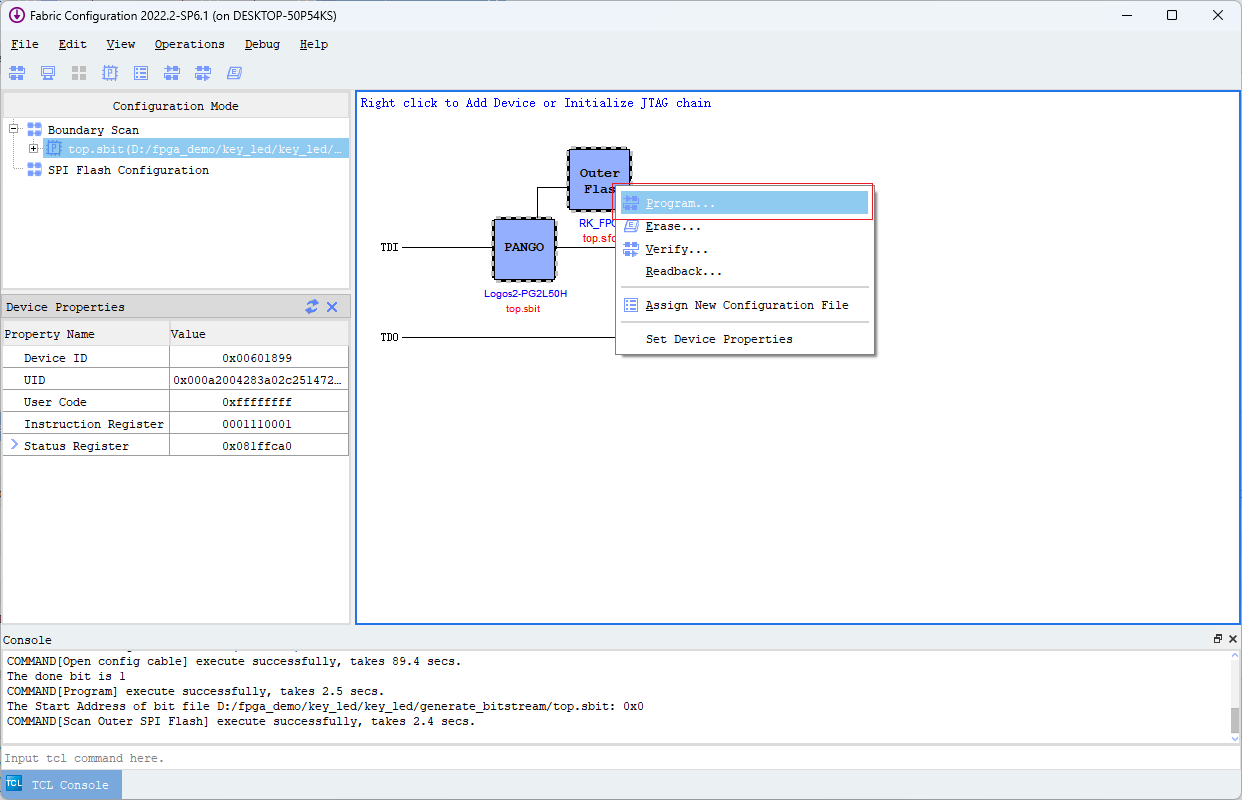
Right-click the position in the figure below, then click Program.
Successful flash programming is shown below:
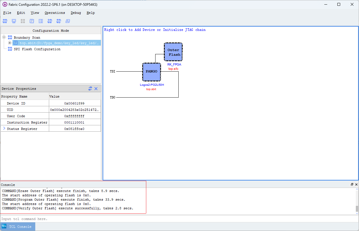
Now power off the board and power it on again. If you can see the corresponding experimental phenomenon when pressing key0 and key1, it means the flashing was successful. (Wait about 15s)
Finally, the on-board result is as follows.
3 Pango Clock Resources — Phase-Locked Loop
3.1 Experiment Introduction
Experiment purpose: Understand the basic usage of the PLL IP. Experiment environment: Window11 PDS2022.2-SP6.4 Chip model: PG2L50H-484
3.2 Experiment Principle
3.2.1 PLL Introduction
As a feedback control circuit, a phase-locked loop is characterized by using an external input reference signal to control the frequency and phase of the oscillation signal inside the loop. Because a phase-locked loop can automatically track the output signal frequency to the input signal frequency, phase-locked loops are usually used in closed-loop tracking circuits. While the phase-locked loop is working, when the frequency of the output signal is equal to the frequency of the input signal, the output voltage and the input voltage maintain a fixed phase difference, i.e., the phase of the output voltage is locked to the input voltage, which is the origin of the name "phase-locked loop".
Phase-locked loops have powerful performance. They can perform arbitrary frequency division, frequency multiplication, phase adjustment, and duty cycle adjustment on the clock signal input to the FPGA, thereby outputting a desired clock. In addition, in some complex projects, even if we don't need to modify any clock parameters, PLLs are often used to optimize clock jitter to obtain a more stable clock signal. It is exactly because these PLL performance characteristics are needed in actual design and cannot be achieved by writing code that the PLL IP core has become one of the most commonly used IP cores in program design.
The PLL IP is an IP designed by Pango based on PLL and clock network resources. Through different parameter configurations, it can realize functions such as frequency adjustment, phase adjustment, synchronization, and frequency synthesis of clock signals.
3.2.2 IP Configuration
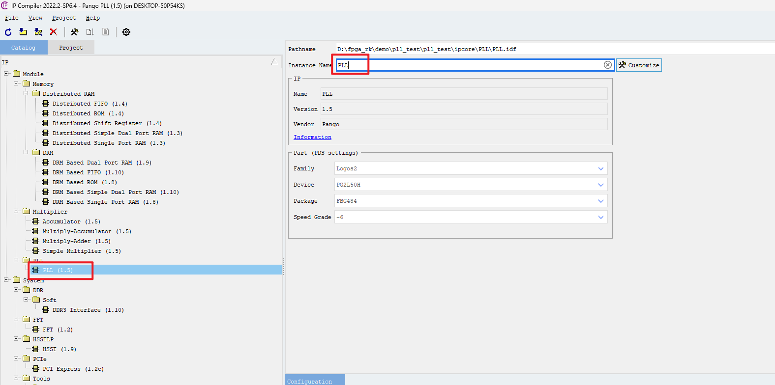
First, click the "IP" icon on the shortcut toolbar to enter the IP instantiation settings.

Then select PLL at the IP directory, give a name to this instantiated IP in Instance name, and then click Customise to enter the IP configuration page. The operation diagram is as follows:
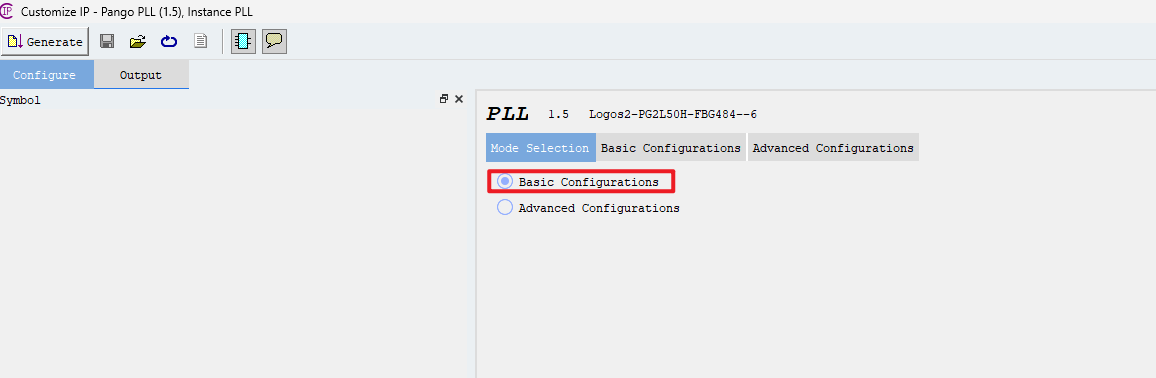
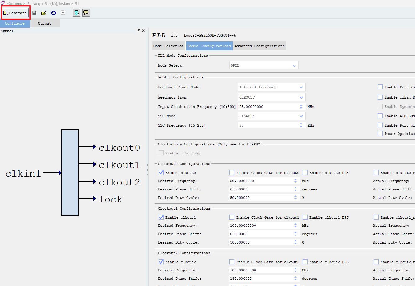
The PLL can be used in two modes: Basic and Advanced. In Advanced mode, the internal parameters of the PLL are fully open. You need to fill in the input division coefficient, output division coefficient, duty cycle, phase, feedback division coefficient, etc., to configure it correctly. In Basic mode, users do not need to care about the PLL's internal parameter configuration; they only need to input the desired frequency value, phase value, duty cycle, etc., and the IP will automatically calculate the optimal configuration parameters. If there is no special application, it is recommended to use the Basic mode to configure the PLL. In this experiment, we select Basic Configuration.
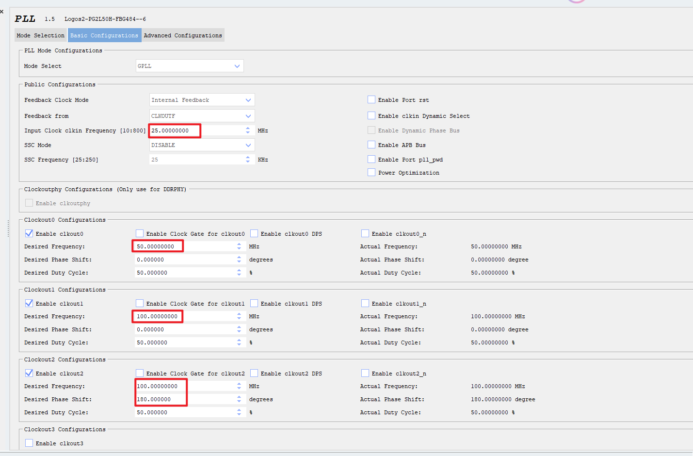
Next, perform the basic configuration:
In the Public Configurations column, set the input clock frequency to 25MHz.
Under the Clockout0 Configurations tab, check to enable clkout0, and set the output frequency to 50MHz.
Under the Clockout1 Configurations tab, check to enable clkout1, and set the output frequency to 100MHz.
Under the Clockout2 Configurations tab, check to enable clkout2, set the output frequency to 100MHz, and set the phase offset to 180 degrees.
Other options can use the default settings. If you have other needs, please refer to the IP manual. This experiment only introduces the basic usage of the IP:
Click Generate in the upper-left corner to generate the IP.
3.3 Code Design
The module interface list is as follows:
PLL IP usage experiment module interface table
| Port | I/O | Width | Description |
|---|---|---|---|
| sys_clk | input | 1 | System clock |
| clkout0 | output | 1 | 54MHz clock |
| clkout1 | output | 1 | 81MHz clock |
| clkout2 | output | 1 | 81MHz clock, phase offset 180 degrees |
| lock | output | 1 | Clock lock signal; when high, it means the IP core output clock is stable. |
PLL_TEST top-level code:
module PLL_TEST(
    input                               sys_clk                    ,
    output                              clkout0                    ,
    output                              clkout1                    ,
    output                              clkout2                    ,
    output                              lock
   );

PLL PLL_U0 (
    .clkout0                            (clkout0                   ),// output
    .clkout1                            (clkout1                   ),// output
    .clkout2                            (clkout2                   ),// output
    .lock                               (lock                      ),// output
    .clkin1                             (sys_clk                   ) // input
);


endmodule
The function of this module is to instantiate the PLL IP core. The function is simple and will not be described here.
PLL_tb test code:
timescale 1ns / 1ps

module    PLL_tb();
    reg                                        sys_clk                    ;
    wire                                       clkout0                    ;
    wire                                       clkout1                    ;
    wire                                       clkout2                    ;
    wire                                       lock                       ;


    initial
        begin
            #2
                    sys_clk <= 0     ;


    parameter   CLK_FREQ = 25;//Mhz
    always # ( 1000/CLK_FREQ/2 ) sys_clk = ~sys_clk ;


PLL_TEST u_PLL_TEST(
    .sys_clk                            (sys_clk                   ),
    .clkout0                            (clkout0                   ),
    .clkout1                            (clkout1                   ),
    .clkout2                            (clkout2                   ),
    .lock                               (lock                      )
);


endmodule
timescale defines the time unit and time precision of the module simulation. The time unit is 1 nanosecond, and the precision is 1 picosecond.
The initial block is responsible for initializing the system clock. Two nanoseconds after the simulation starts, the system clock sys_clk is set to 0. This is to define a known initial state at the beginning of the simulation.
The code defines a clock frequency parameter CLK_FREQ of 25 MHz, and uses an always block to toggle the system clock signal. The logic in the always block toggles sys_clk every 40 nanoseconds, thereby generating a 25 MHz square-wave clock signal. This clock signal is used to drive the PLL_TEST module under test.
Finally, each signal of the testbench is connected to the PLL_TEST module. This includes connecting the generated system clock sys_clk to the clock input of PLL_TEST, and using wire to bring out the output signals clkout0, clkout1, clkout2, and lock of PLL_TEST for observation.
3.4 PDS and Modelsim Co-Simulation
PDS supports co-simulation with third-party simulators such as Modelsim or QuestaSim. Modelsim is the more commonly used simulator, so we use PDS and Modelsim for co-simulation.
Next, select Project->Project Setting, open the project settings, and prepare to set up co-simulation.
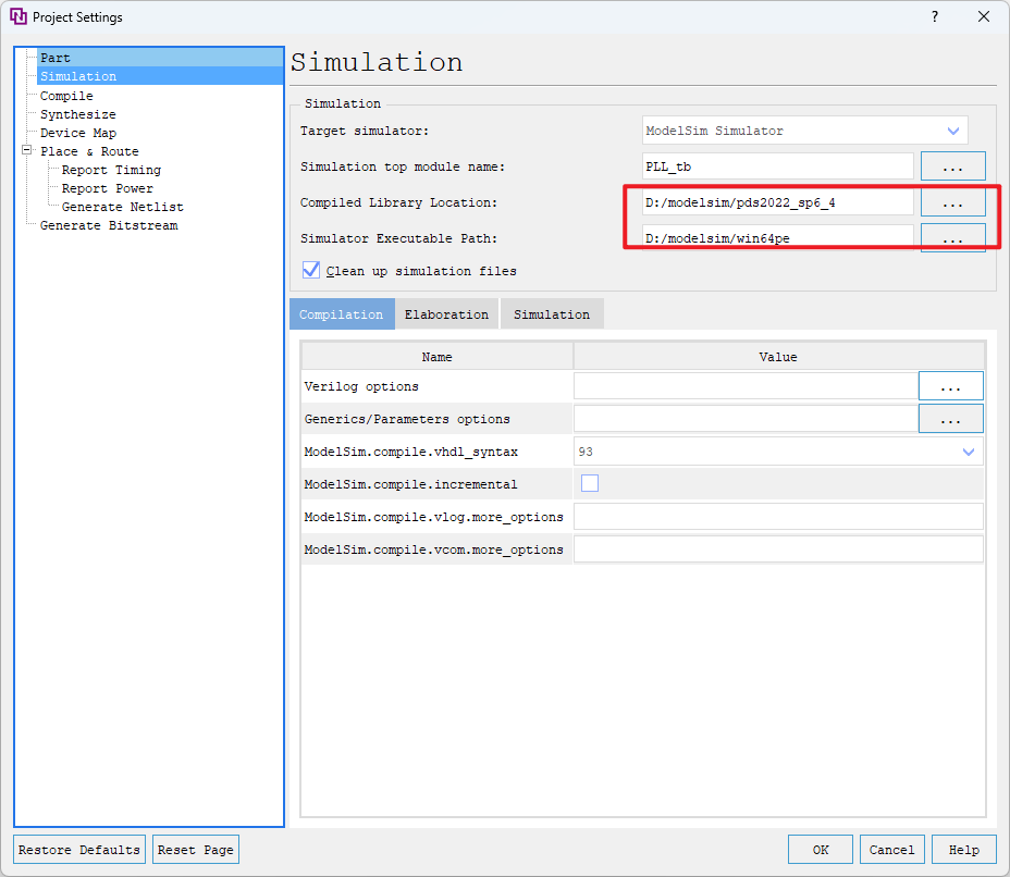
Select the Simulation tab. Red box 1 selects the path of the simulation library just compiled, and red box 2 selects the Modelsim startup path. Then click OK.
Right-click the simulated file and select Run Behavior Simulation to start behavioral simulation.
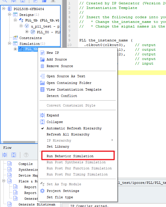
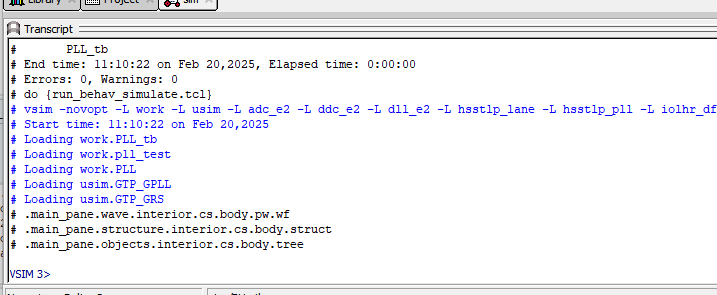
After running, Modelsim will open automatically and perform the simulation. If there are no errors, it means success. If errors occur, please check the configuration of PDS and Modelsim.
3.5 Experiment Phenomenon
Click Wave to observe the PLL output signals:
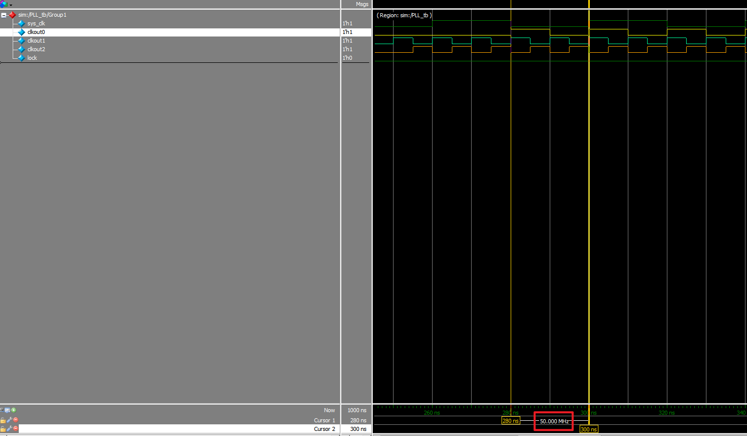
Using the ruler to measure clkout0, we find its one clock period is 20ns, which is 50MHz.
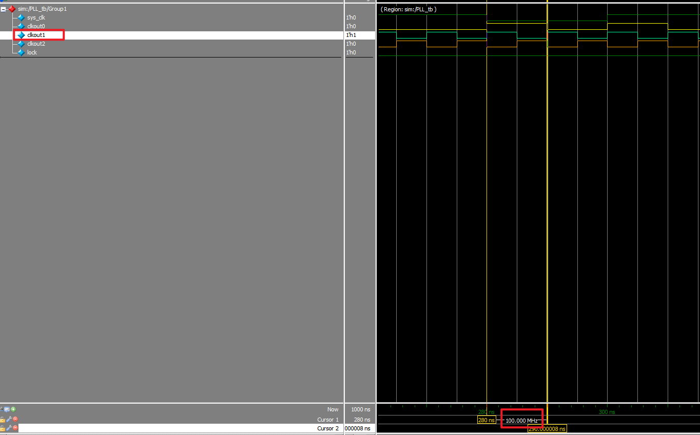
You can see that the clkout1 clock frequency is 100MHz, and it has a 180° phase difference from clkout2, consistent with the settings. Note that the PLL output clock should be used only after the clock lock signal lock is valid. The clock output before the lock signal goes high is undefined.
4 Using RAM, ROM, and FIFO
4.1 Experiment Introduction
Experiment purpose: Master the use of RAM, ROM, and FIFO IPs on the Pango platform. Experiment environment: Window11 PDS2022.2-SP6.4 Chip model: PG2L50H-484
4.2 Experiment Principle
Whether it is the Logos series or the Logos2 series, their IP configuration, modes, and functions are all the same. Unlike the PLL, which has choices like dynamic configuration and internal feedback options, RAM, ROM, and FIFO are universal.
4.2.1 RAM Introduction
RAM is random access memory. It can write data to any address during operation, and can also read data from any address. Its role can be used for data caching, cross-clock-domain, or storing intermediate algorithm computation results.
Note that the PDS IP configuration tool provides two different RAMs: one is Distributed RAM and the other is DRM Based RAM. Distributed RAM uses LUT (lookup table) resources to form the RAM. This kind of RAM consumes a lot of LUT resources, so it is usually used for relatively small storage to save DRM resources. DRM Based RAM uses on-chip DRM resources to form the RAM, does not occupy logic resources, and is fast. DRM Based RAM is usually used in designs.
RAM is divided into three types, as shown in the following table:
| RAM Type | Characteristics |
|---|---|
| Single-port RAM | Only one port can read and write. It has only one read/write port and address port |
| Pseudo dual-port RAM | Has two ports, wr and rd. As the name implies, wr can only write, and rd can only read |
| True dual-port RAM | Provides two ports, A and B; both ports can independently read and write |
Note that when using a true dual-port, you should avoid reading and writing the same address at the same time, which will cause the write to fail. This situation should be avoided in logic design.
The following shows a commonly used RAM configuration as an introduction. Usually, we use pseudo dual-port RAM for design, as shown in the figure below:
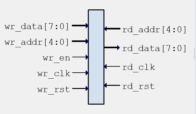
The following figure shows the IP configuration:
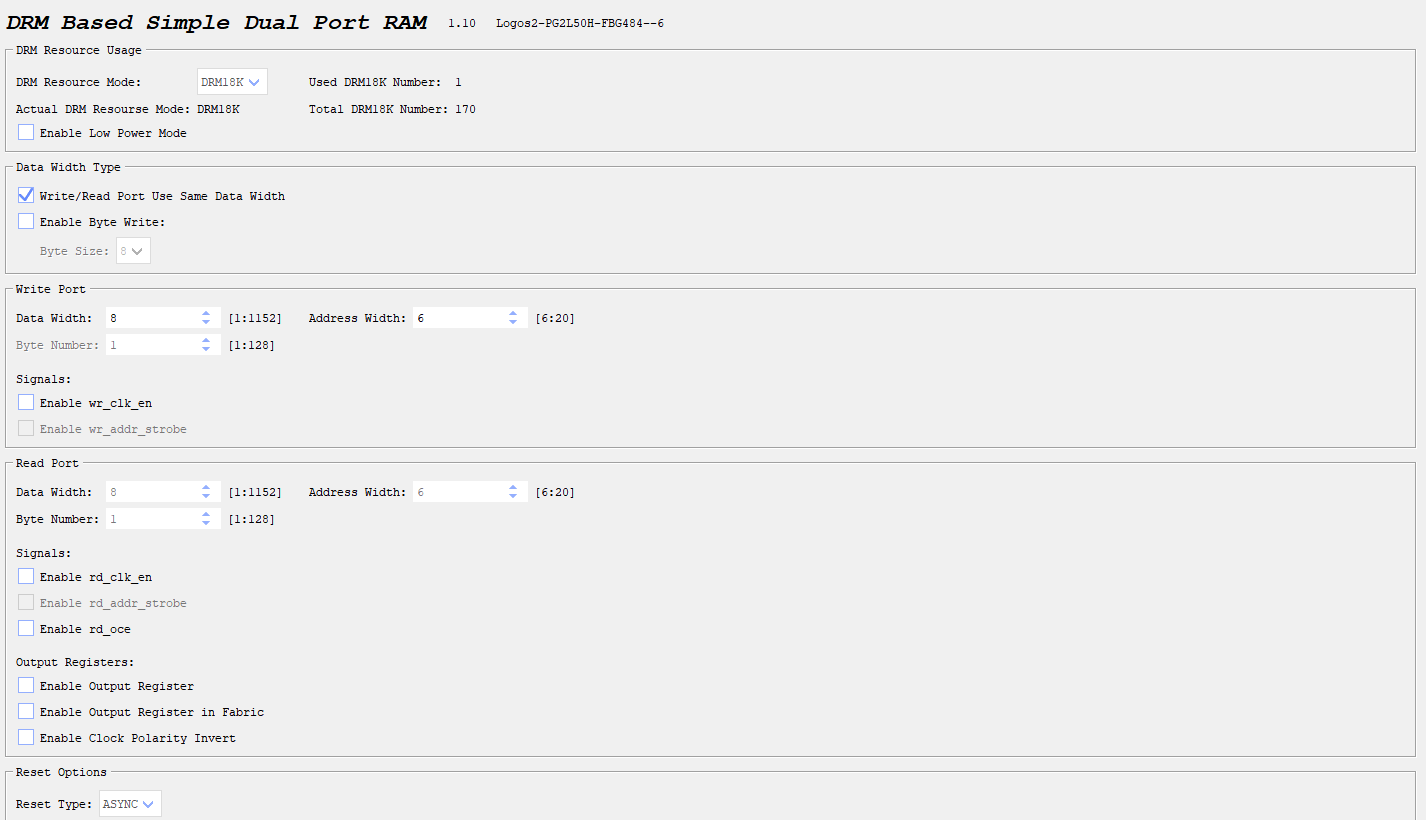
Note that if Enable Output Register (output register) is checked, the output data will be delayed by one clock cycle.
For the specific meaning of each port, please refer to the official manual. You can also view the IP manual yourself, as shown in the figure below:
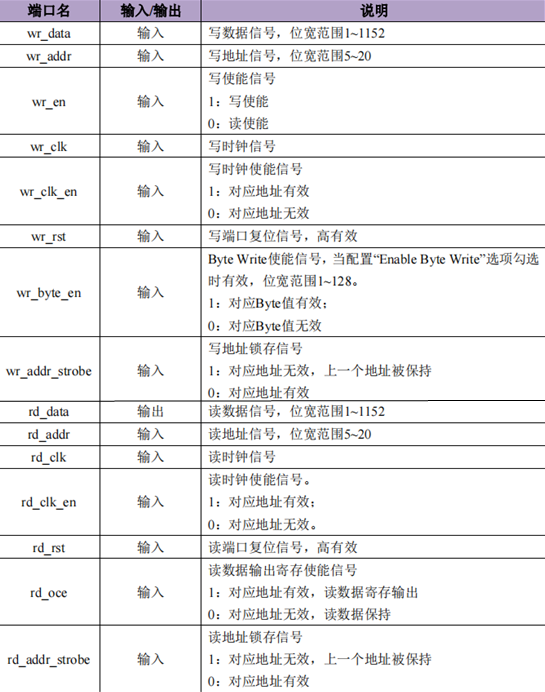
DRM Resource Type: Used to configure which resource the RAM IP core uses. The resources available for different chip models are different — some are 9K, some are 18K, and some are 36K. If there are no special circumstances, just use AUTO.
4.2.1.1 RAM Read/Write Timing
When configured in different modes, the RAM read/write timing is different. True dual-port and single-port RAM configurations have three modes, while pseudo dual-port has only one. Since the configurations of true dual-port and single-port are the same, here we use true dual-port as an example.
There are three modes: NORMAL_WRITE (normal mode), TRANSPARENT_WRITE (direct write), and READ_BEFORE_WRITE (read-priority mode).
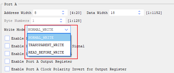
The pseudo dual-port does not belong to the above three modes; it has its own unique mode. The difference between these modes lies in the read/write timing. Next, let's analyze the read/write timing.
The following timing diagrams all come from the official IP manual, and none of them enable the output register. Note that wr_en=1 means write data, and wr_en=0 means read data.
(1) NORMAL_WRITE
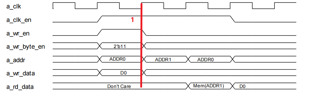
In NORMAL_WRITE mode, you can see that when the clock rising edge arrives, and both clk_en and wr_en are high, the data is written to the corresponding address, as at moment 1 in the figure. Then look at the read data port. When wr_en is not 0, a_rd_data is always in the Don't Care state. When the clock rising edge arrives, clk_en is high, and wr_en is low, a_rd_data outputs the data in the current a_addr, i.e., Mem(ADDR1) and D0 in ADDR0.
(2) READ_BEFORE_WRITE
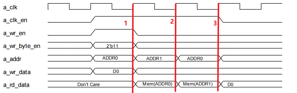
In READ_BEFORE_WRITE mode, you can see that at moment 1, the clock rising edge arrives, and both clk_en and wr_en are high. D0 is written into ADDR0. But note that a_rd_data and a_addr at this time: you can find that a_wr_en is not 0, yet a_rd_data still outputs the data of ADDR0 from the previous moment (because it is not outputting D0). Afterwards, a_wr_en goes low, and now it's reading data. At moment 3, the data of ADDR0 is read out, and a_rd_data outputs D0.
So to summarize, this mode actually means that when a write operation is performed, the read port outputs the original data of the currently written address. Therefore, calling it "read priority mode" makes sense — as the name implies, it gives priority to reading out the original data.
(3) Transparent_Write
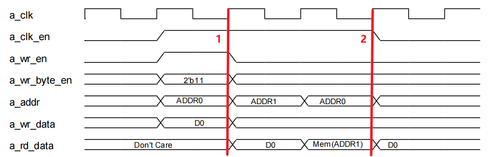
In Transparent_Write mode, you can see that at moment 1, the clock rising edge arrives, and both clk_en and wr_en are high. D0 is written into ADDR0. But note that a_rd_data and a_addr at this time: you can find that a_wr_en is not 0, yet a_rd_data directly outputs D0. Then a_wr_en goes low, entering the read state. At moment 2, the data of ADDR0 is read out again, and D0 is output.
To analyze and summarize, based on the situation at moment 1, we can conclude that in this mode, when we perform a write operation, the read port immediately outputs the data we write. So it is called direct-write mode.
(4) Pseudo Dual-Port Read/Write Timing
Note: wr_en=1 is a write operation, and wr_en=0 is a read operation.
The pseudo dual-port read/write timing is different from the above three. Let's analyze the following timing diagram:
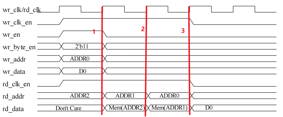
Note moment 1. At this time, both wr_en and wr_clk_en are high, so it's a write operation. At moment 1, D0 is written to address ADDR0. Note the rd_addr and rd_data at this moment. You can see that rd_addr is ADDR2 at this moment, and during the write operation, rd_data also outputs the data in ADDR2, while wr_en is still high. Next, look at moments 2 and 3. At this time, wr_en is 0 and rd_clk_en is high, so it's a read operation. At this time, the data in ADDR1 and ADDR0 are read out respectively. Then rd_clk_en goes low, the read clock becomes invalid, and rd_data keeps outputting D0.
To analyze and summarize, mainly moment 1: you can see that at moment 1, D0 is written to ADDR0, but the read port outputs the data in ADDR2. Careful observation leads to the conclusion: when the pseudo dual-port RAM performs a write operation, it outputs the data of the address the read port currently points to. Is it a bit like direct write? Except that direct write outputs the written data, while the pseudo dual-port outputs the data of the address the read port points to.
2.1.1.2 ROM Introduction
ROM is read-only memory. During program execution, it can only be read and cannot be written. Therefore, we should configure its initial value at initialization. Generally, the initial value is configured by importing a .dat file when generating the IP.
Note that the PDS IP configuration tool provides two different ROMs: one is Distributed ROM and the other is DRM Based ROM. Distributed ROM uses LUT (lookup table) resources to form the ROM. This kind of ROM consumes a lot of LUT resources, so it is usually used for relatively small storage to save DRM resources. DRM Based ROM uses on-chip DRM resources to form the ROM, does not occupy logic resources, and is fast. DRM Based ROM is usually used in designs.
The following shows a commonly used ROM configuration as an introduction. Since it can only be read, it is a single-port ROM, as shown in the figure below:

The following figure shows the IP configuration:
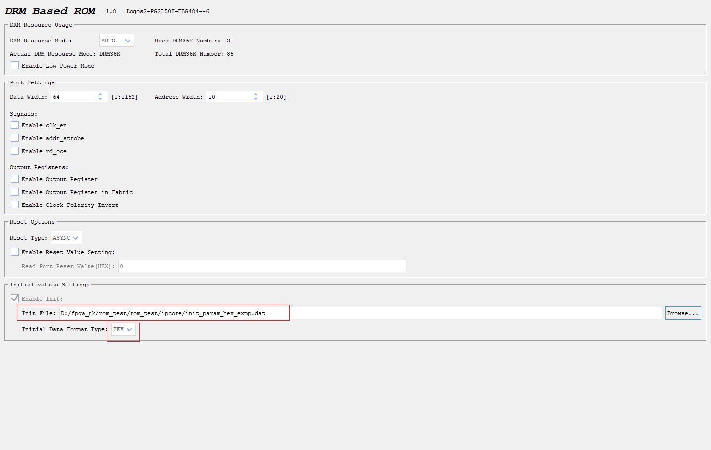
Note that if Enable Output Register (output register) is checked, the output data will be delayed by one clock cycle.
At the same time, you can see that the Enable Init option is checked by default and cannot be unchecked.
The format of the imported data can only be binary or hexadecimal. The demo uses hexadecimal.
For the specific meaning of each port, please refer to the official manual. You can also view the IP manual yourself, as shown in the figure below:
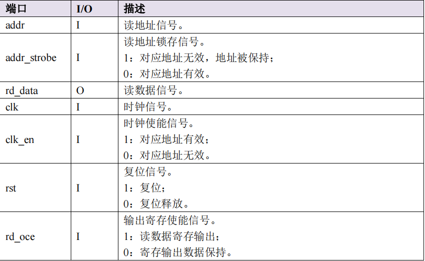
Generally, we only need four signals: addr, rd_data, clk, and rst.
The following timing diagrams all come from the official IP manual, and none of them enable the output register.
4.2.1.2 ROM Read Timing
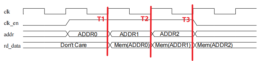
You can see that the timing is very simple. For example, at moment TI, when the clk rising edge arrives and clk_en is high, if you provide the address to be read, rd_data will output the data. When the output enable register is not checked, rd_data output will be delayed; the specific time can be seen from the simulation. So we can only get the value read from the ROM at the rising edge of the next clock cycle, i.e., the rising edge of moment T2.
So the overall timing is very simple. If you check the clk_en signal, you must give clk_en a high level to read data. If you do not check the clk_en signal, the ROM data is continuously read according to the address.
4.2.2 FIFO Introduction
FIFO is first-in-first-out. In an FPGA, the role of FIFO is to provide a buffer with first-in-first-out characteristics for stored data, and it is often used for data caching or cross-clock-domain data transmission. The biggest difference between FIFO and RAM is that FIFO does not need an address; it uses sequential write-in and sequential read-out.
In Pango's IP tool, there are Distribute FIFO and DRM FIFO, which are actually composed of different resources. The former Distribute FIFO, also called distributed FIFO, is composed of on-chip LUT resources, while DRM FIFO is composed of on-chip DRM resources. The FIFO composed of DRM has better performance than that composed of LUT resources — not only larger capacity but also more configurable functions.
This chapter focuses on DRM Based FIFO.
Note: After a FIFO is full, do not continue to write data, otherwise write overflow will occur.
Note: After a FIFO is empty, do not continue to read data, otherwise read overflow will occur.
The following shows a commonly used FIFO configuration as an introduction.
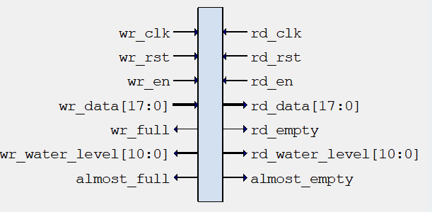
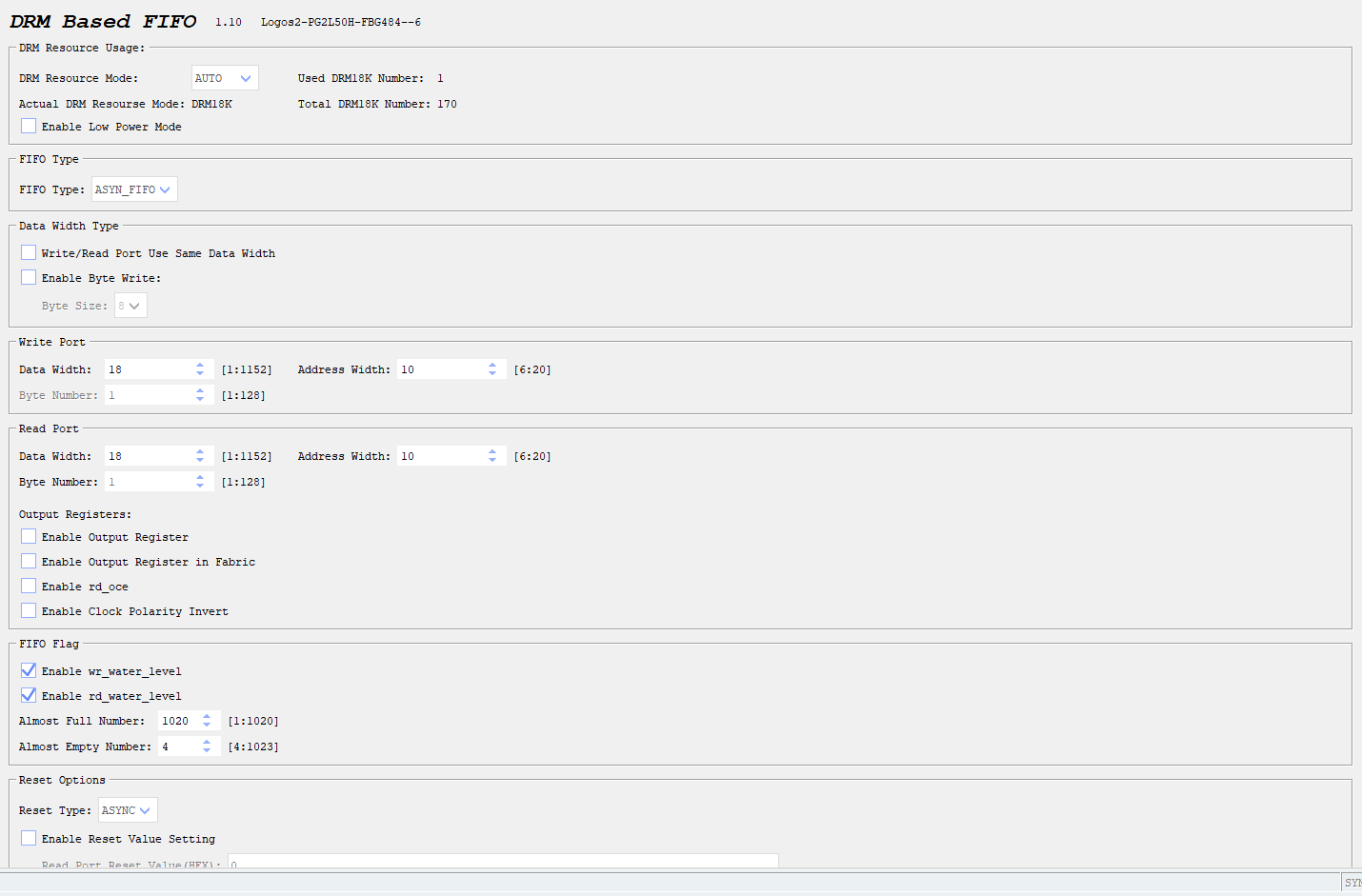
Note that if Enable Output Register (output register) is checked, the output data will be delayed by one clock cycle.
FIFO Type has two types: SYNC and ASYNC. The first is a synchronous FIFO, where the read and write ports share a clock and reset. The other is an asynchronous FIFO, where the read/write clocks and resets are independent. In normal design, asynchronous FIFO is more commonly used, because the read/write timing of synchronous FIFO and asynchronous FIFO is exactly the same; only the clock/reset of the read/write ports differs. When the read/write ports of an asynchronous FIFO use the same clock and reset, the asynchronous FIFO and the synchronous FIFO are basically the same.
Reset Type can also be SYNC or ASYNC. In SYNC mode, the rising edge of the clock needs to sample the active reset before resetting. In ASYNC mode, once there is a reset, the FIFO resets immediately.
For the description of other ports, refer to the official IP manual, as shown in the figure below:
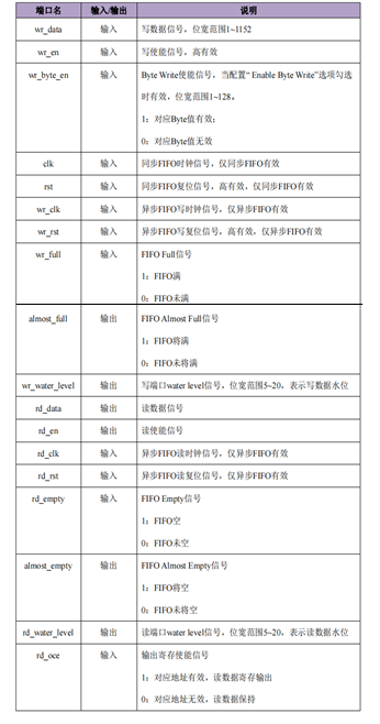
Among them, rd_water_level and wr_water_level respectively represent "the amount of readable data" and "the amount of data already written". Their meaning is the same as the wr_data_count and rd_data_count of Xilinx's FIFO.
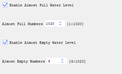
When we check Enable Almost Full Water Level and Enable Almost Empty Water Level, we can see rd_water_level and wr_water_level. The Almost Full Numbers setting means that when 1020 pieces of data are written, the Almost Full signal goes high. The Almost Empty Numbers setting means that when there are 4 pieces of readable data left, the Almost Empty signal goes high.
FIFO also supports mixed bit widths, e.g., a 16-bit write port and an 8-bit read port. If 16'h0102 is written, then it will be read out as 8'h02, 8'h01 — the low bits are read out first.
If the write port is 8-bit and the read port is 16-bit. When 8'h01 and 8'h02 are written, the readout is 16'h0201 — the data written first is stored in the low bits.
4.2.2.1 FIFO Read/Write Timing
Because the read/write timing of synchronous FIFO and asynchronous FIFO is the same, here we use the asynchronous FIFO read/write timing diagram for the introduction.
Note: The reset is active high. None of the read-out data enables Enable Output Register (output register).
(1) Write Timing When FIFO Is Not Full
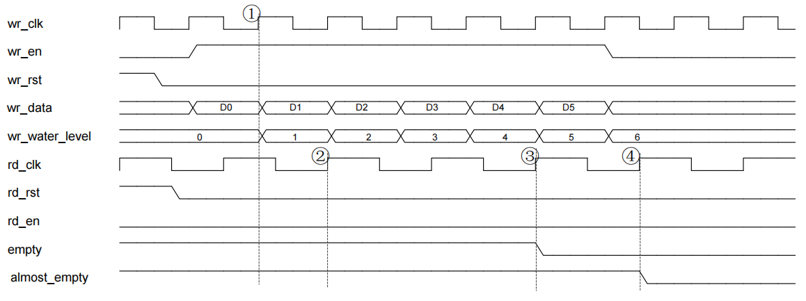
You can see that at moment 1, the reset signal is low, in the working state. At this time, when the rising edge of wr_clk arrives and wr_en is high, data D0 is written into the FIFO. wr_water_level also changes from 0 to 1, indicating that one piece of data has been written. At this time, look at the empty signal of the read port. At moment 3, the empty signal changes from high to low, meaning that the read port already has data to read and the FIFO is no longer empty. Note that rd_clk and wr_clk are different. From writing at moment 1 to the empty signal going low at moment 3, 3 rd_clks have passed.
So here we can conclude: rd_water_level lags wr_water_level by three rd_clks.
(2) Write Timing When FIFO Is Almost Full
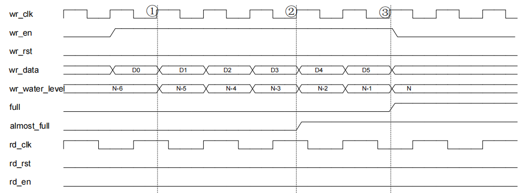
When almost full, we mainly analyze the full and almost_full signals. Suppose Almost Full Numbers is set to N-2. At moment 1, N-6 pieces of data have been written, which means writing 6 more pieces will fill the FIFO. From moment 1 to moment 2, 4 pieces of data are written. So when wr_water_level becomes N-2, the condition is met, and you can see the Almost Full signal go high. Writing 2 more pieces of data fills the FIFO, so after another two clock cycles, the Full signal goes high.
(3) Read Timing When FIFO Is in the Full State
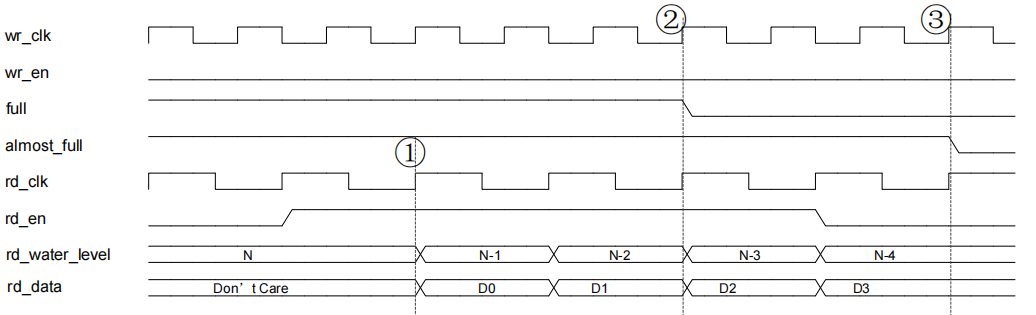
In the full state, the FIFO already has N pieces of data. At moment 1, when the rd_clk rising edge arrives and rd_en is high, data is read out from the FIFO (the data output has a delay; in the simulation, the delay is 0.2ns). At this time, rd_water_level becomes N-1, and rd_data outputs D0. Then look at moment 2: the full signal goes low. Note that from moment 1 to moment 2, 3 wr_clks have passed before the write port can judge that the amount of data is no longer full. So we can conclude that wr_water_level lags rd_water_level by three wr_clks.
(4) Read Timing When FIFO Is Almost Empty
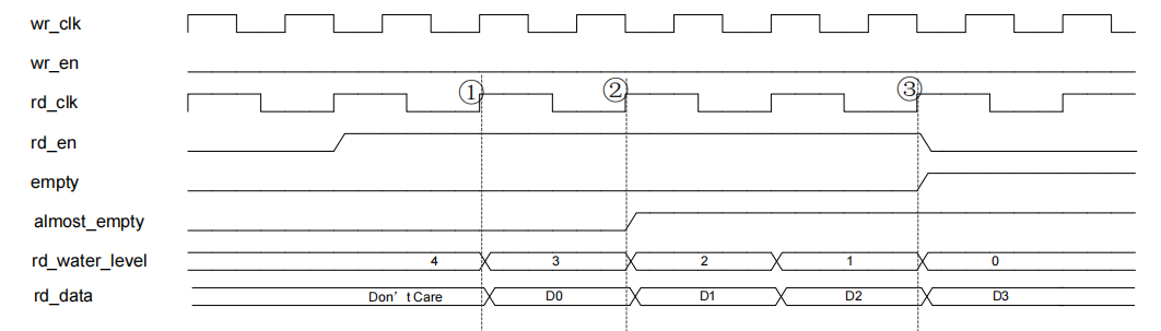
At moment 1, there are 4 pieces of readable data left. Suppose Almost Empty Number is set to 2. At moment 1 and moment 2, two pieces of data are read out respectively. So at moment 2, there are 2 pieces of readable data left, which meets the Almost Empty Number trigger condition. Therefore, the almost_empty signal goes high. After two more clock cycles, i.e., reading two more pieces of data, the FIFO becomes empty, which is state 3. At this time, the empty signal goes high.
2.1.2 Interface List
This section introduces the interface of each top-level module.
ram_test_top.v
| Port | I/O | Width | Description |
|---|---|---|---|
| wr_clk | input | 1 | Write clock |
| rd_clk | input | 1 | Read clock |
| rst_n | input | 1 | Global reset |
| rw_en | input | 1 | 1: write operation 0: read operation |
| wr_addr | input | 5 | Write address |
| rd_addr | input | 5 | Read address |
| Wr_data | input | 8 | Data written to RAM |
| Rd_data | output | 8 | Data read out from RAM |
rom_test_top.v
| Port | I/O | Width | Description |
|---|---|---|---|
| rd_clk | input | 1 | Read clock |
| rst_n | input | 1 | Global reset |
| rd_addr | input | 10 | Read address |
| rd_data | input | 64 | Data read out from ROM |
fifo_test_top.v
| Port | I/O | Width | Description |
|---|---|---|---|
| sys_clk | input | 1 | Write/read clock |
| rst_n | input | 1 | Global reset |
| wr_addr | input | 8 | Data written to FIFO |
| wr_en | input | 1 | Write enable |
| rd_en | input | 1 | Read enable |
| wr_water_level | output | 8 | Amount of data already written to FIFO |
| rd_water_level | output | 8 | Amount of data readable from FIFO |
| Rd_data | output | 8 | Data read out from FIFO |
4.3 Project Description
None
4.4 Code Simulation Description
This time the top-level module actually just instantiates the IP and brings out the ports, so the main code is in the testbench. We directly introduce the simulation code.
4.4.1 RAM Simulation Test
`timescale	1ns/1ns
module	ram	test	tb()
reg	sys	clk
reg	rd	clk
reg	rst	n
reg	rw	en	//读写使能信号

reg	[7:0]	wr	data
reg	[4:0]	wr	addr
reg	[4:0]	rd	addr

wire	[7:0]	rd	data

reg	[1:0]	state

initial
begin
rst	n	<=	1'd0
sys	clk	<=	1'd0
rd	clk	<=	1'd0
#20
rst	n	<=	1'd1

end

//读写控制
always@(posedge	sys	clk	or	negedge	rst	n)	begin
if(!rst	n)
begin
state	<=	2'd0
wr	data	<=	8'd0
rw	en	<=	1'd0
wr	addr	<=	8'd0
rd	addr	<=	8'd0
end
else
begin
case(state)
2'd0:begin
rw	en	<=	1'd1
state	<=	2'd1
end

2'd1:begin
if(wr	addr	==	5'd31)
begin
rw	en	<=	1'd0
state	<=	2'd2
wr	data	<=	8'd0
wr	addr	<=	5'd0
rd	addr	<=	5'd0
end
else
begin
state	<=	2'd1
wr	data	<=	wr	data+1'b1
rd	addr	<=	rd	addr+1'b1
wr	addr	<=	wr	addr+1'b1
end
end
2'd2:begin
if(rd	addr	==	5'd31)
begin
state	<=	2'd3
rd	addr	<=	5'd0
end
else
begin
state	<=	2'd2
rd	addr	<=	rd	addr+1'b1
end
end
2'd3:begin
state	<=	2'd0
end

default:	state	<=	2'd0
endcase
end
end

//50MHZ
always#10	sys	clk	=	~sys	clk

//
GTP	GRS	GRS	INST(
GRS	N(1'b1)
)

ram	test	top	u	ram	test	top(
wr	clk	(	sys	clk	"),"
rd	clk	(	sys	clk	"),"
rst	n	(	rst	n	"),"
rw	en	(	rw	en	"),"
wr	addr	(	wr	addr	"),"
rd	addr	(	rd	addr	"),"
wr	data	(	wr	data	"),"
rd	data	(	rd	data	)
)
endmodule
The basic operations related to tb will not be described in detail here; we only focus on the key logic parts. Lines 27 to 80 of the code are the RAM read/write control state machine, mainly used to control the generation of read/write addresses and enables and the data written. Here we only explain the main implemented functions. First, in lines 38-42 of the code, i.e., when state=0, rw_en is pulled high and jumps to state 1, entering the write operation (clk_en is not enabled, so it can be ignored). Data starts to be written in the next clock cycle (note that this is sequential logic, sampled at the edge, so writing starts in the next clock cycle), i.e., when state=1, data is continuously written into the RAM. In lines 44 to 60 of the code, this is the write operation. You can see that when wr_addr is not equal to 31, wr_data and wr_addr keep incrementing by 1 (rd_addr is incremented by 1 here; you can refer to the video explanation, mainly to verify the pseudo dual-port timing). When wr_addr equals 31, the data is cleared in the next clock cycle, and the state jumps. In the current clock cycle, data will continue to be written to address 31, so in this clock cycle, 32 pieces of data are written in total (from address 0 to address 31). That is, state 1 jumps to state 2's logic after writing 32 pieces of data. In lines 61-72 of the code, i.e., when state=2, rd_addr keeps incrementing at the rising edge of each cycle until rd_addr=31. In the next clock cycle, the address is cleared and the state jumps, while in the current clock cycle, the data at address 31 continues to be read out, completing the reading of data from addresses 0-31, a total of 32 pieces of data. So this state mainly completes reading 32 pieces of data, and then jumps to state 3 in the next clock cycle. In state=3, you can see that its main role is to wait one clock cycle, and then jump back to state=0, playing a delay role.

The figure above is the waveform of the written data. The data increments from 0 to 31, and the addresses also go from 0 to 31.

The figure above is the read data waveform. 0-31 pieces of data are read from addresses 0-31.
For the specific waveform, you can refer to the video simulation, or try simulating yourself, and look at the code according to the waveform. Because this is sequential logic, if you are a beginner, you may be confused about why one more piece of data is read at the moment rd_addr=31 by just reading the text. It is recommended to simulate directly or watch the simulation part of the video explanation to help you quickly understand.
We can summarize in one sentence: the assignment of sequential logic always takes effect in the next clock cycle. Therefore, the operation performed when rd_addr=31 will only be sampled and take effect in the next clock cycle. So the current clock will still read one more piece of data from the RAM.
4.4.2 ROM Simulation Test
`timescale 1ns/1ns
module rom_test_tb();
reg    sys_clk;
reg    rst_n;
reg    [9:0]    rd_addr;
wire   [63:0]    rd_data;

initial
begin
    rst_n    <=    1'd0;
    sys_clk  <=    1'd0;
    #20
    rst_n    <=    1'd1;

end

//50MHZ
always#10 sys_clk = ~sys_clk;
//
GTP_GRS GRS_INST(
    .GRS_N(1'b1)
    ) ;

always@(posedge sys_clk or negedge rst_n)    begin
    if(!rst_n)
        rd_addr    <=    10'd0;
    else
        rd_addr    <=    #2 rd_addr + 1'b1;
end

rom_test_top u_rom_test_top(
    .rd_clk   ( sys_clk  ),
    .rst_n    ( rst_n    ),
    .rd_addr  ( rd_addr  ),
    .rd_data  ( rd_data  )
);

endmodule
Lines 31-36 of the code instantiate the ROM top-level module. The module actually just calls the ROM IP and brings out the signals to ports without any logic operations.
Lines 24-29 use an always block to continuously generate addresses and provide them to the ROM IP to read out data. Since clk_en is not checked, data is continuously read out after the ROM reset completes. So there is no complex logic; it just increments the address from 0 continuously and reads out the data.

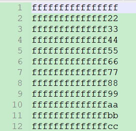
The figure above is the waveform of the read-out data. You can see that the read-out data is consistent with the data in the dat file.
4.4.3 FIFO Simulation Test
`timescale	1ns/1ns
module	fifo_test_tb();

reg	sys_clk;
reg	rst_n;

reg	[7:0]	wr_data;
reg	wr_en;
reg	rd_en;

reg	rd_state;	//读状态
reg	wr_state;

wire	[7:0]	rd_data;
reg	[7:0]	rd_cnt;

wire	[7:0]	rd_water_level;
wire	[7:0]	wr_water_level;

initial
begin
rst_n	<=	1'd0;
sys_clk	<=	1'd0;
#20
rst_n	<=	1'd1;


end

always#10	sys_clk	=	~sys_clk;	//50MHZ

always@(posedge	sys_clk	or	negedge	rst_n)	begin
if(!rst_n)
begin
wr_state	<=	1'd0;
wr_en	<=	1'd0;
wr_data	<=	8'd0;
end
else
begin
case(wr_state)
1'd0:	if(wr_water_level	==	127)	//128个数据
begin
wr_en	<=	#2	1'd0;
wr_data	<=	#2	8'd0;
wr_state	<=	#2	1'd1;
end
else
begin
wr_en	<=	#2	1'd1;
wr_data	<=	#2	wr_data+1'b1;
wr_state	<=	#2	1'd0;
end

1'd1:	if(rd_cnt	==	127)
wr_state	<=	#2	1'd0;


default:	wr_state	<=1'd0;
endcase
end
end

always@(posedge	sys_clk	or	negedge	rst_n)	begin
if(!rst_n)
begin
rd_state<=	1'd0;
rd_en	<=	1'd0;
rd_cnt	<=	8'd0;
end
else
begin
case(rd_state)
1'd0:	if(rd_water_level	>=	8'd128)	//等待128个数据
begin
rd_state	<=	#2	1'd1;
rd_en	<=	#2	1'd1;
end
else
begin
rd_cnt	<=	#2	8'd0;
rd_state	<=	#2	1'd0;
end

1'd1:	begin

rd_cnt	<=	#2	rd_cnt	+	1'b1;
if(rd_cnt	==	127)
begin
rd_en	<=	#2	1'd0;
rd_state	<=	#2	1'd0;
end
end
default:	rd_state	<=	1'd0;
endcase
end
end

GTP_GRS	GRS_INST(
GRS_N(1'b1)
)	;

fifo_test_top	u_fifo_test_top(
sys_clk	(	sys_clk	"),"
rst_n	(	rst_n	"),"
wr_data	(	wr_data	"),"
wr_en	(	wr_en	"),"
rd_en	(	rd_en	"),"
wr_water_level	(	wr_water_level	"),"
rd_water_level	(	rd_water_level	"),"
rd_data	(	rd_data	)
);
endmodule
The basic operations related to tb will not be described in detail here; we only focus on the key logic parts. The whole design is divided into the control of two states: read and write. They respectively complete writing 128 pieces of data and reading 128 pieces of data. Since FIFO doesn't need addresses, only enable signals need to be generated.
First, look at the write state. When wr_state=0, the write enable is pulled high, wr_data keeps incrementing, and data is written into the FIFO. When wr_water_level=127, the write enable is pulled low, the write data is set to 0, and the write state jumps to 1. Note that at this time, one more piece of data will be written, so a total of 128 pieces of data are written. The operations of pulling the write enable low, setting the write data to 0, and jumping the write state to 1 will be sampled and take effect in the next clock cycle. After that, in wr_state=1, it keeps waiting for rd_cnt. This condition determines that when 128 pieces of data are read out, wr_state jumps back to state 0.
Next, look at the read state. In rd_state=0, once the amount of readable data reaches 128 (including 128), the state jumps to rd_state=1, and then data starts to be read out. At the same time, in rd_state=1, a variable rd_cnt is used to count the read-out data. rd_cnt starts counting from 0. When rd_cnt=127, one more piece of data will be read out from the FIFO, so a total of 128 pieces of data are read out. In the next clock cycle, both rd_en and rd_state will be set to 0.

The waveform of the written data is shown above. A total of 128 pieces of data are written, from 1 to 128.

The waveform of the read-out data is shown above. A total of 128 pieces of data are read out, from 1 to 128.
For the specific waveform, you can refer to the video simulation, or try simulating yourself, and look at the code according to the waveform. Because this is sequential logic, if you are a beginner, you may be confused about why one more piece of data is read at the moment rd_cnt=127 by just reading the text. It is recommended to simulate directly or watch the simulation part of the video explanation to help you quickly understand.
We can summarize in one sentence: the assignment of sequential logic always takes effect in the next clock cycle. So the operation performed when rd_cnt=127 will only be sampled and take effect in the next clock cycle. So in the current clock, rd_en is still 1, and one more piece of data will be read out from the FIFO.
5 DDR3 Read/Write Experiment Routine
5.1 Experiment Introduction
Experiment purpose: Complete the DDR3 read/write test. Experiment environment: Window11 PDS2022.2-SP6.4 Chip model: PG2L50H-484
5.2 Experiment Principle
The development board integrates one 4Gbit (512MB) DDR3 chip, model MT41K256M16. The total bus width of DDR3 is 16bit. The maximum data rate of DDR3 SDRAM is 1066Mbps.
5.2.1 DDR3 Controller Introduction
PG2L50H provides users with a complete DDR memory controller solution with flexible configuration. It uses a soft core to implement DDR memory control and has the following features:
- Supports DDR3
- Supports x8, x16 Memory Device
- Maximum bit width supports 32 bit
- Supports simplified AXI4 bus protocol
- One AXI4 256 bit Host Port
- Supports Self_refresh, Power down
- Supports Bypass DDRC
- Supports DDR3 Write Leveling and DQS Gate Training
- Maximum DDR3 rate up to 1066 Mbps
5.3 Project Description
After PDS is installed, you need to manually add the DDR3 IP. Please complete the following steps:
DDR3 IP file: PG2L_IP\PG2L_IP\DDR3\ips2l_hmic_s_v1_10.iar

5.3.1 DDR3 Read/Write Example Project
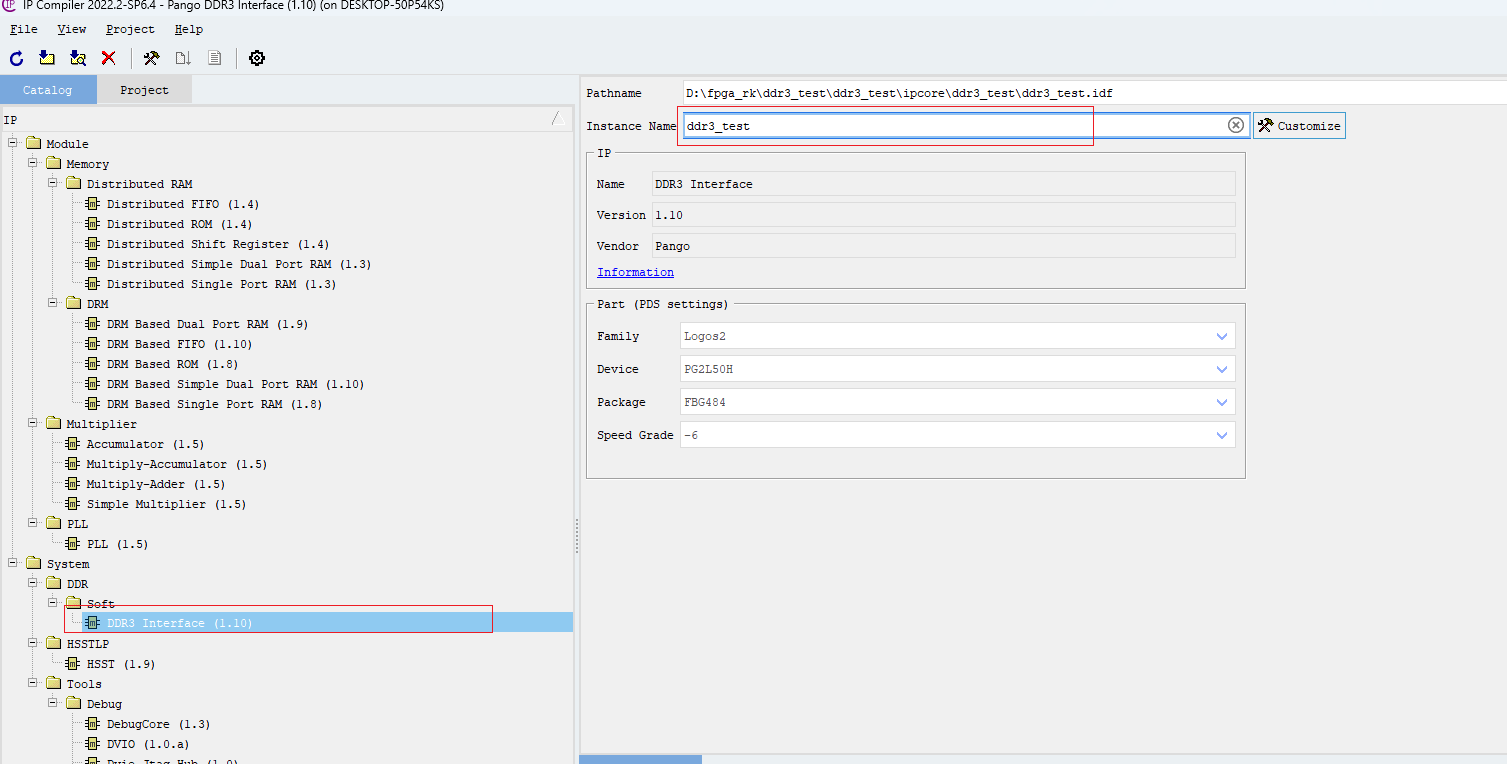
Open the PDS software, create a new project ddr3_test, click the icon below to open the IP Compiler;

Select the DDR3 IP, name it ddr3_test, and then click Customize;
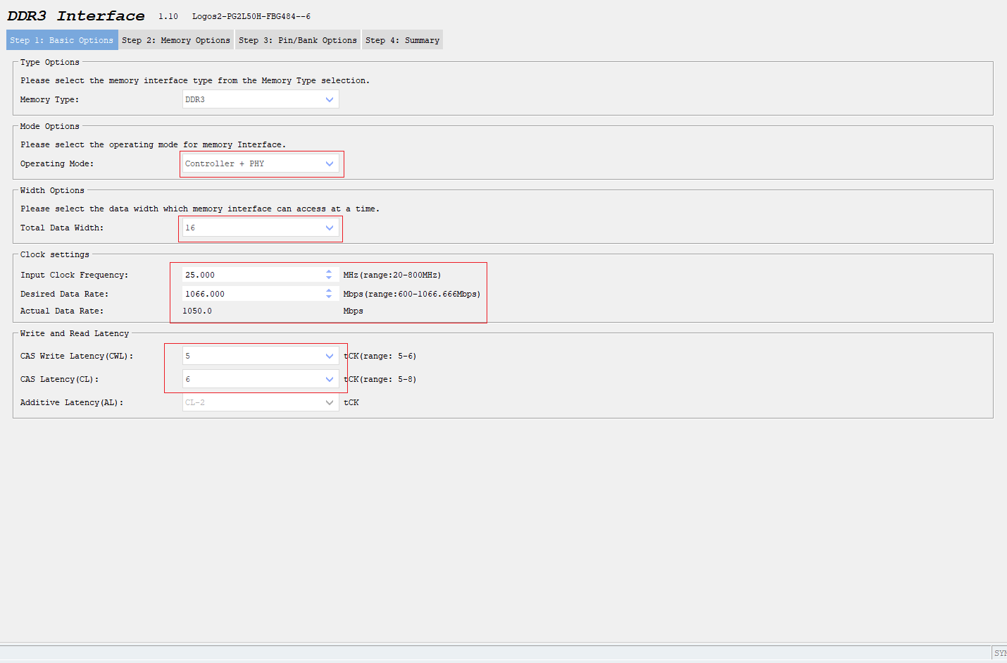
In the DDR3 settings interface, set Step1 as follows:
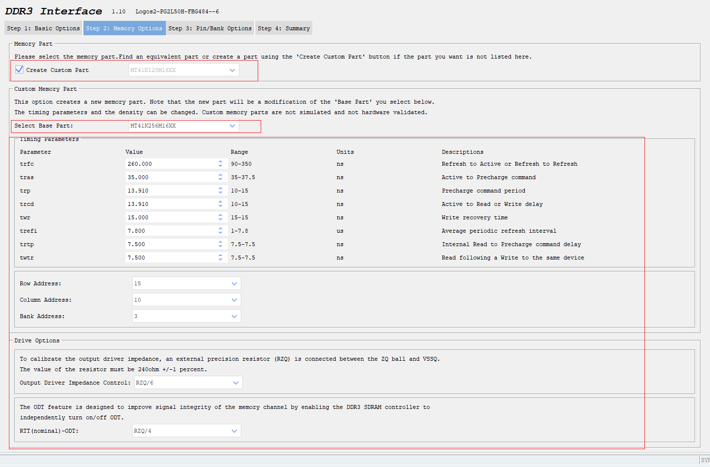
Set Step2 as follows. You need to create a new DDR3 model, select MT41K256M16XX as the template, and keep the Timing parameters and address and Drive Options consistent with the settings in the figure below.
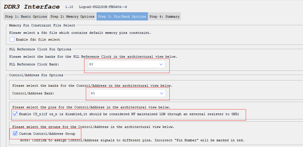
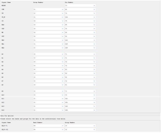
Set Step3 as follows, check Custom Control/Address Group, and refer to the schematic for pin constraints:
Reminder:
When setting the IP core, in step 3: pin/bank options, the correspondence between Group Number in the pin settings and the schematic is shown in the figure below.

R5 represents BANK5, and G1 represents Group Number 1.

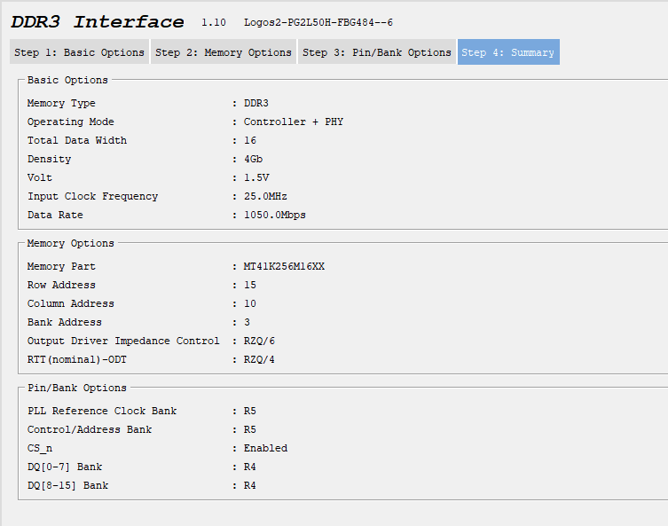
Step4 is a summary. Click Generate to generate the DDR3 IP;
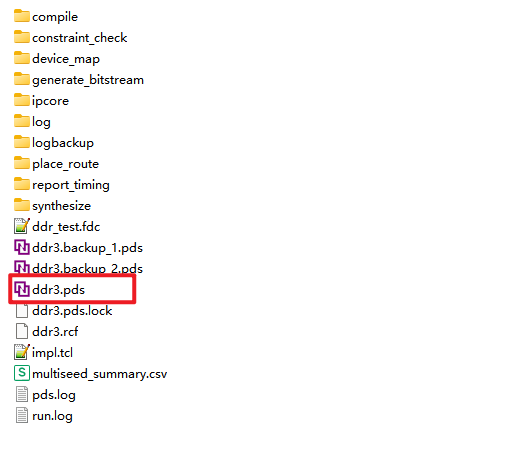
Close this project and open the Example project from this path:
Xxxxx\ddr3_test\ip_core\ddr3\pnr
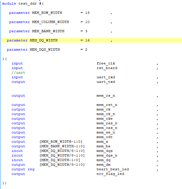
Open the top-level file. The top-level file needs to be modified. For details, refer to the detailed code. The figure below shows the modified top-level file.
For pins other than those already constrained in "Step3", use the UCE tool to modify them according to the schematic. For porting, you can directly refer to the project's fdc file for porting.
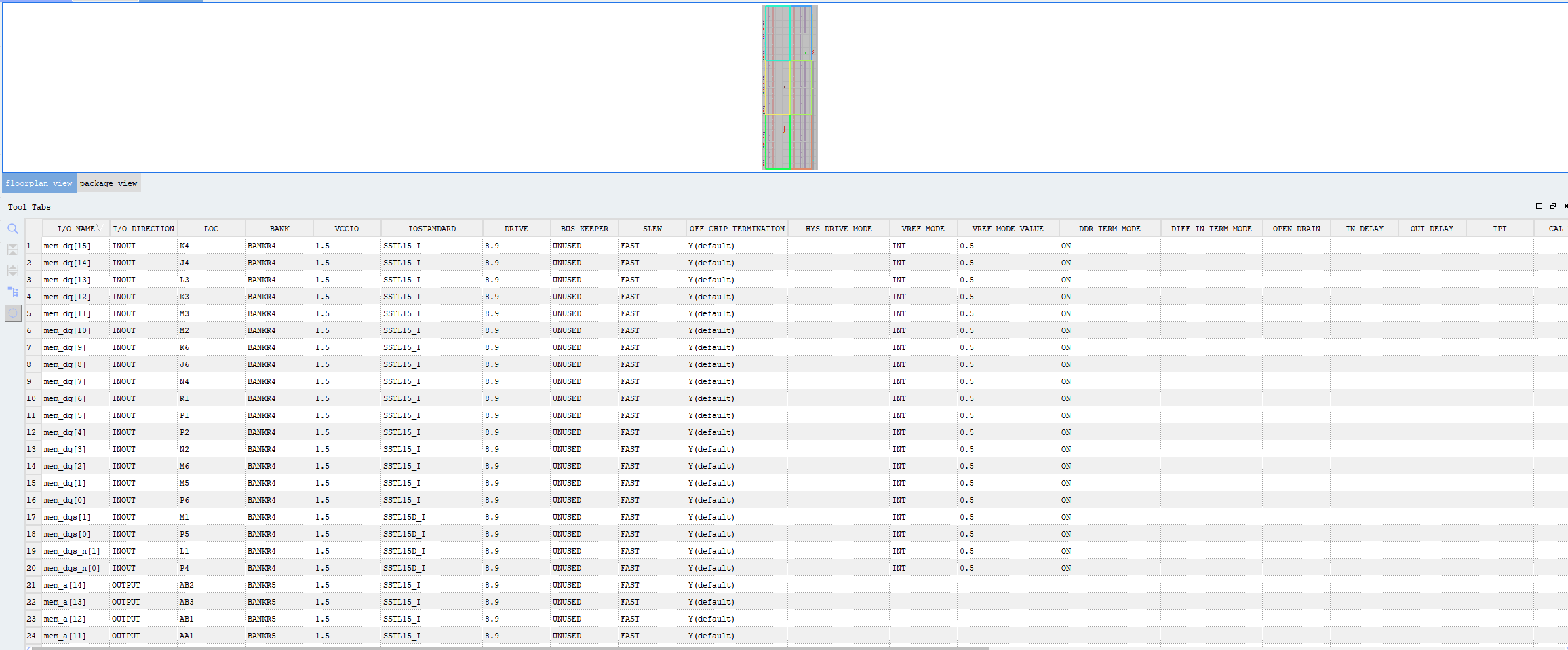
The following pins can be constrained to LEDs for easy observation of the experimental phenomenon;

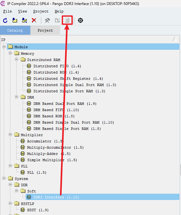
You can view the IP core's user guide in the following way to understand the Example module composition;
5.4 Experiment Phenomenon
Download the program. You can see LED1 is always on, LED3 blinks, LED4 blinks, and LED5 is always on;
| Signal Name | Reference Description | LED Number |
|---|---|---|
| err_flag_led | Data check error signal | 3 |
| heart_beat_led | Heartbeat signal | 4 |
Reminder:
The Heart_beat_led signal blinking indicates that the ddrphy system clock is normal.

The err_flag_led signal blinking indicates that the data check has no errors. It can be found in the IP core data manual.

If normal, err_flag_led blinks faster than heart_beat_led.
6 Optical Fiber Communication Test Experiment Routine
6.1 Experiment Introduction
Experiment purpose: Realize data transmission and reception between optical modules through optical fiber connection.
Experiment environment: Window11 PDS2022.2-SP6.4 Chip model: PG2L50H-484
6.2 Experiment Principle
PG2L100H has a built-in high-speed serial interface module with line rates up to 6.6Gbps, namely HSSTLP, which contains 1 HSSTLP with a total of 4 full-duplex transceiver LANEs. In addition to PMA, HSSTLP also integrates rich PCS functions and can be flexibly applied to various serial protocol standards. Inside the product, each HSST supports 1-4 full-duplex transceiver LANEs. The main features of HSST include:
- Supports DataRate: 0.6Gbps-6.6Gbps
- Flexible reference clock selection
- Independent configuration of transmit and receive channel data rates
- Programmable output swing and de-emphasis
- Receiver adaptive linear equalizer Logos2 series FPGA device data manual
- PMA Rx supports SSC
- Data channel supports data widths: 8bit only, 10bit only, 8b10b, 16bit only, 20bit only, 32bit only, 40bit only, 64b66b/64b67b and other modes
- Flexibly configurable PCS, supporting protocols such as PCI Express GEN1, PCI Express GEN2, XAUI, Gigabit Ethernet, CPRI, SRIO, etc.
- Flexible Word Alignment function
- Supports RxClock Slip function to ensure fixed Receive Latency
- Supports protocol standard 8b10b encoding/decoding
- Supports protocol standard 64b66b/64b67b data adaptation function
- Flexible CTC scheme
- Supports x2 and x4 Channel Bonding
- HSSTLP configuration supports dynamic modification
- Near-end loopback and far-end loopback modes
- Built-in PRBS function
- Adaptation
6.3 Project Description
6.3.1 Installing the HSST IP Core
After PDS is installed, you need to manually add the HSST IP. Please complete the following steps:
(1) HSST IP file: select 1_9.iar

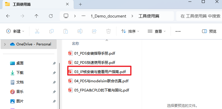
(2) IP installation steps: see "Tool Usage \ 03_IP Core Installation and Viewing the User Guide"
6.3.2 Optical Fiber Communication Test Routine
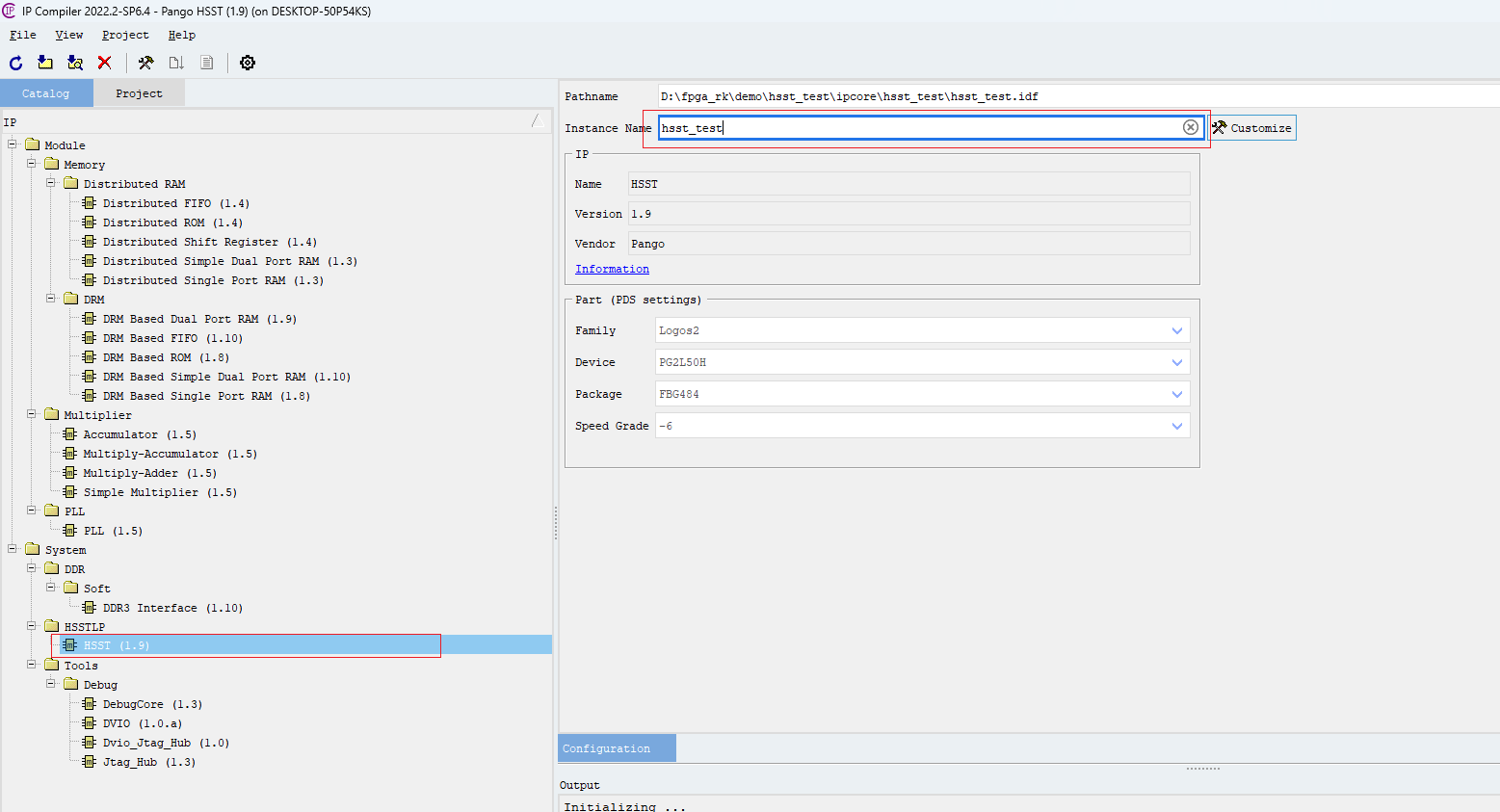
Open the PDS software, create a new project hsst_test, click the icon below to open the IP Compiler;

Select the HSST IP, name it, and then click Customize;
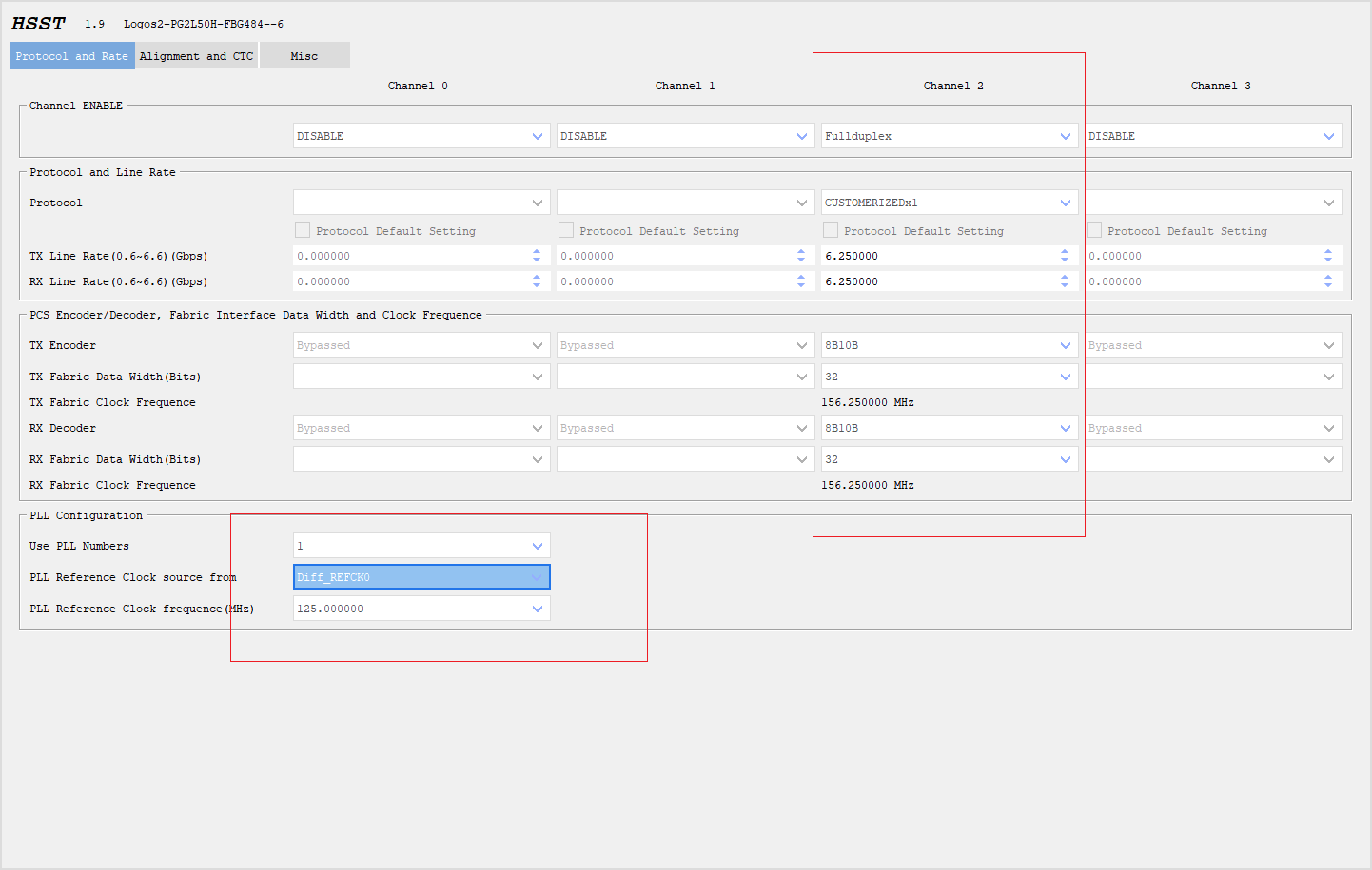
In the HSST settings interface, set Protocol and Rate as follows. Channel0, Channel1, and Channel3 are DISABLE, and Channel2 is set to Fullduplex (full duplex). Protocol selects CUSTOMERIZEDX1 (custom mode). Both TX Line Rate and RX Line Rate select 6.25Gbps. Encoder selects 8B10B. Data Width selects 32bit. The clock selects Diff_REFCK0, and select 125MHz.
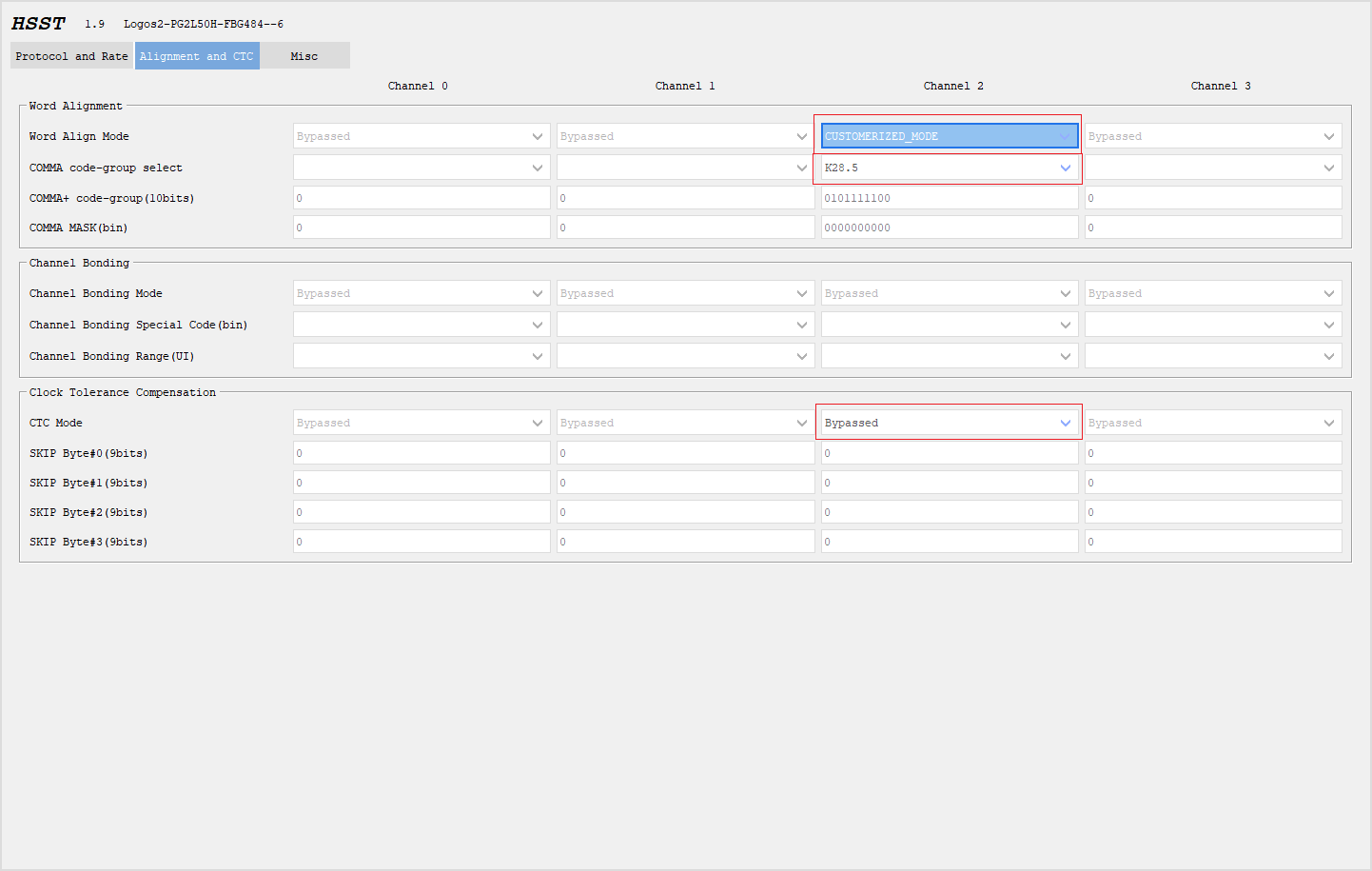
Set Alignment and CTC as follows. Word Align Mode selects CUSTOMERIZED_MODE. The control word (COMMA code-group select) selects K28.5. CTC_MODE selects Bypassed.
Set Misc as follows. The clock selects 25MHz, keep the rest as default, and then click Generate to generate the HSST IP;
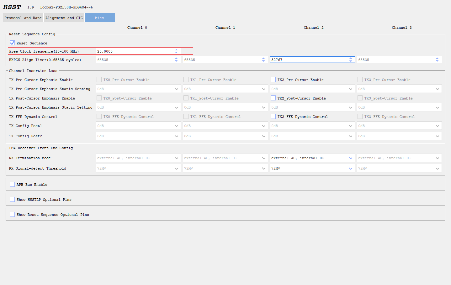
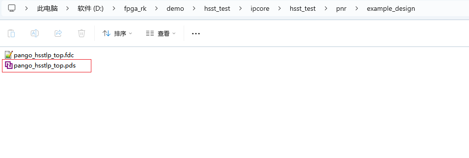
Close this project and open the Example project from this path: hsst_test\hsst_test\ipcore\hsst_test\pnr\example_design
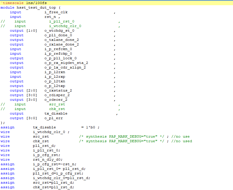
To run on the development board, the reset of the top-level file hsst_test_dut_top needs to be modified. For details, please refer to the routine top-level file:
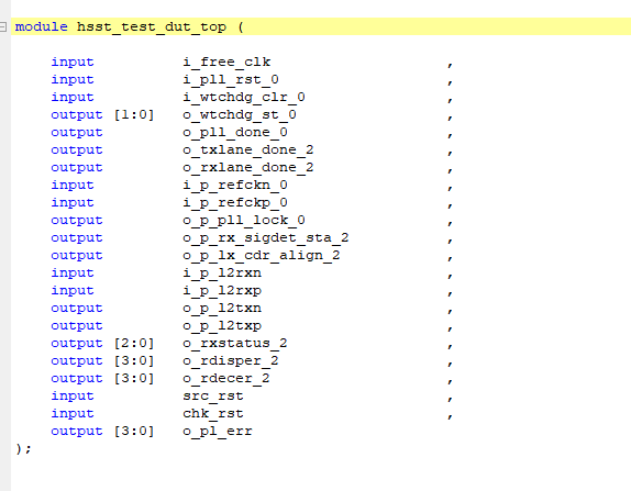
The figure above is the top-level file before modification.
The figure below is the modified top-level file. tx_disable needs to be pulled low to turn on the SFP transmit function.
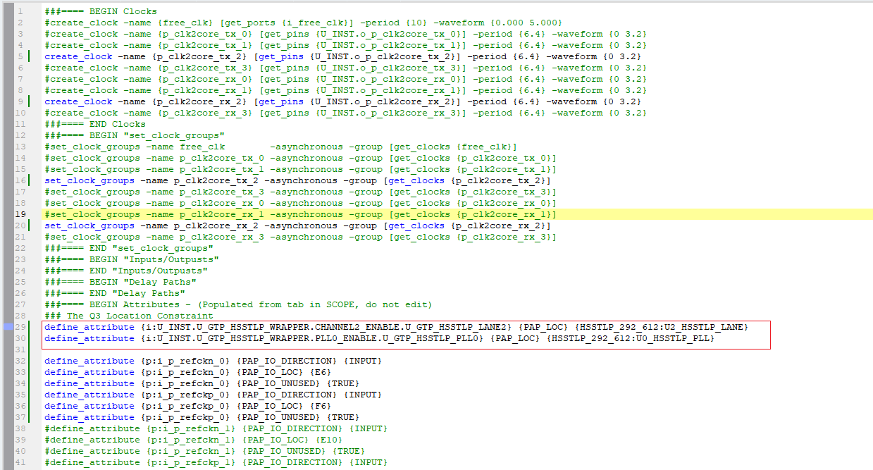
The figure above shows part of the pin constraints. For details, please refer to the project's fdc file. Note that the parts in the red box in the figure are the location constraints of hsst_lane and hsst_pll, which must be added. The differential data pins do not need to be constrained. The reference clock provided to hsst must be constrained, i.e., (i_p_refckn_0 and i_p_refckp_0).
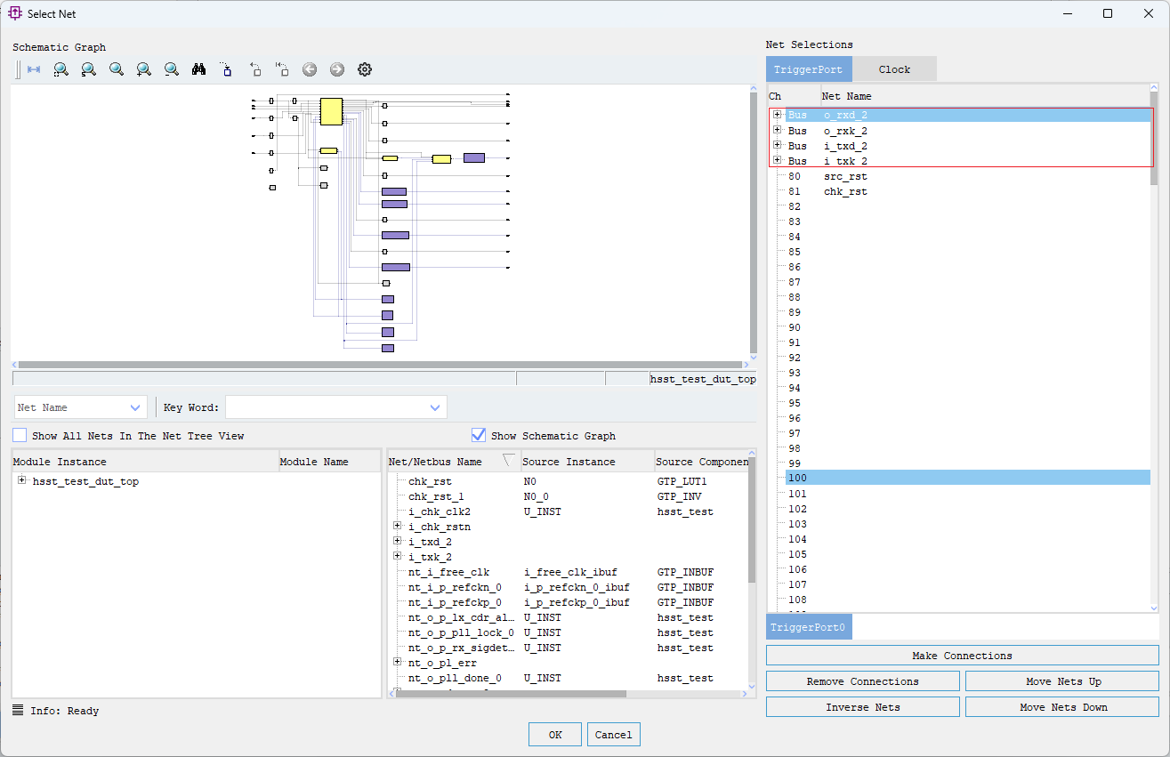
To observe whether there are errors in the transmitted and received data, you need to perform the Debugger insert-core operation.

The clock selects o_p_clk2core_tx_2.
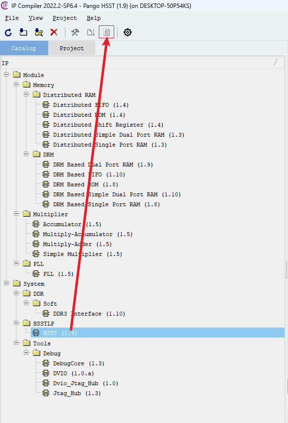
You can view the IP core's user guide in the following way to understand the Example module composition;
6.4 Experiment Phenomenon
Note: Routine location: hsst_test\hsst_test\ipcore\hsst_test\pnr\example_design
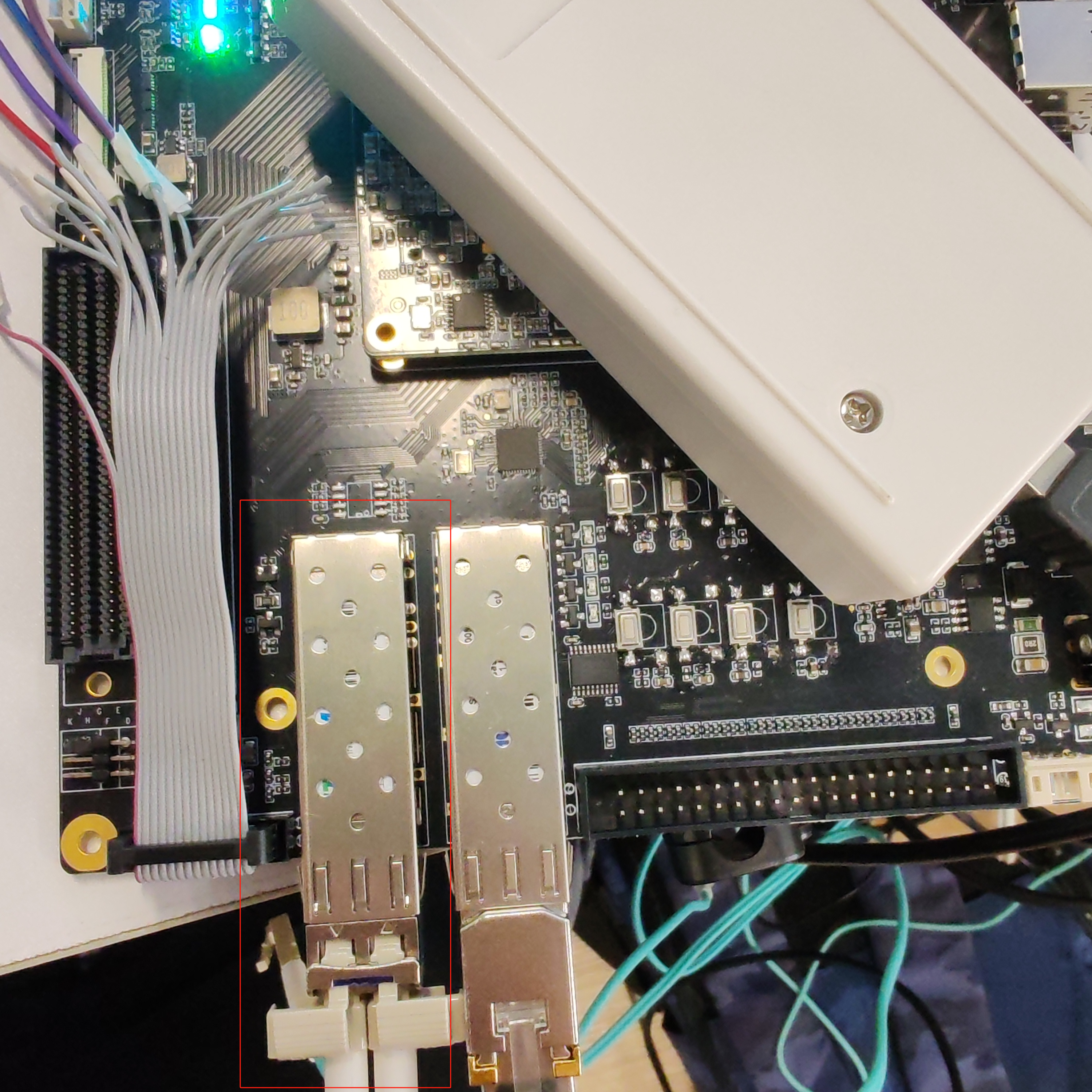
Plug the two ends of the optical fiber into the SFP port (users need to purchase an optical module), and perform Debugger online debugging. You can see that the data sent and received in the window are consistent.
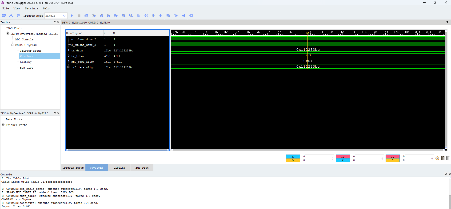
Observe tx_data and rx0_data_align. If they are the same, there is no problem with transmission and reception.
7 Ethernet Transmission Experiment Routine
7.1 Experiment Introduction
Experiment purpose: Complete the Ethernet communication test. Experiment environment: Window11 PDS2022.2-SP6.4 Hardware environment: PG2L50H-484
7.2 Experiment Principle
7.2.1 Development Board Ethernet Interface Introduction
The development board uses a 10/100/1000 Ethernet port implemented by the YT8521SH-CA. When in use, a photoelectric conversion module is required. Connect the computer's network port to the electrical port of the photoelectric conversion module via a network cable to complete the communication.
7.2.2 Ethernet Protocol Introduction
7.2.2.1 Ethernet Frame Format
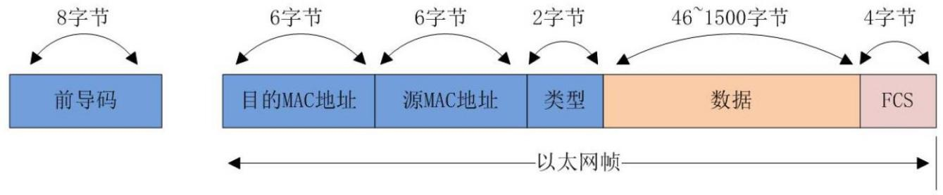
Preamble: 8 bytes, 7 consecutive 8'h55 followed by 1 8'hd5, indicating the start of a frame, used for synchronization between both parties and device data.
Destination MAC address: 6 bytes, storing the physical address of the destination device, i.e., MAC address; Source MAC address: 6 bytes, storing the physical address of the sending device;
Type: 2 bytes, used to specify the protocol type. Common ones are 0800 for IP protocol, 0806 for ARP protocol, and 8035 for RARP protocol;
Data: 46 to 1500 bytes, minimum 46 bytes; if insufficient, it needs to be padded to 46 bytes. For example, the IP protocol layer is included in the data part, including its IP header and data.
FCS: frame tail, 4 bytes, called the frame check sequence, using 32-bit CRC check, checking from the destination MAC address field to the data field.
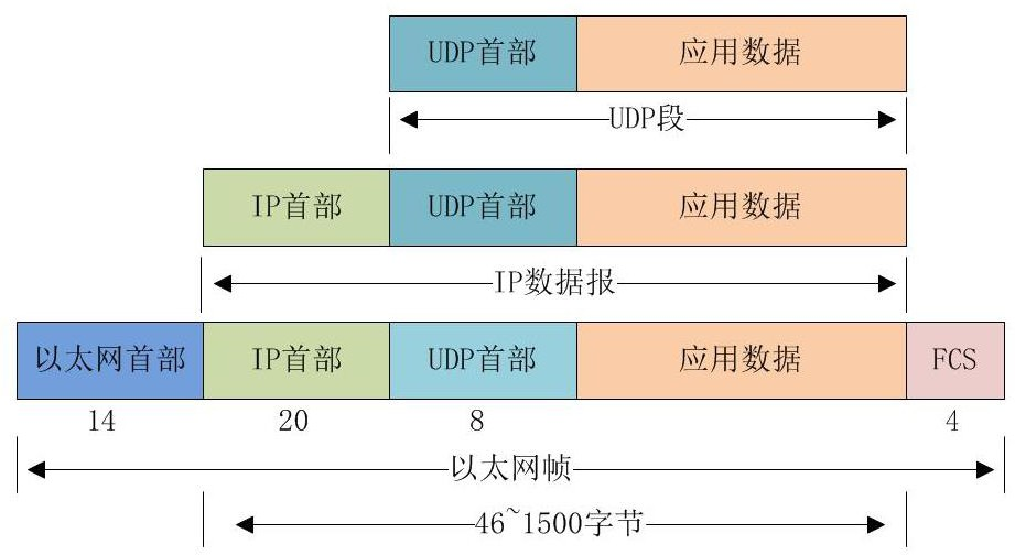
Going further, taking the UDP protocol as an example, we can see its structure is as follows. In addition to the 14 bytes of the Ethernet header, the data part contains the IP header, UDP header, and application data, totaling 46-1500 bytes.
7.2.2.2 ARP Datagram Format
ARP Address Resolution Protocol, i.e., ARP (Address Resolution Protocol), obtains the physical address based on the IP address. The host sends an ARP request broadcast containing the destination IP address (MAC address is 48'hff_ff_ff_ff_ff_ff) to the hosts on the network and receives the returned message to determine the target's physical address. After receiving the returned message, it saves the IP address and physical address to the cache and keeps them for a period of time. Next time it makes a request, it directly queries the ARP cache to save resources. The figure below shows the ARP datagram format.

Frame type: ARP frame type is two bytes 0806;
Hardware type: refers to the link-layer network type, 1 is Ethernet;
Protocol type: refers to the address type to be converted. Use 0x0800 IP type; the subsequent hardware address length and protocol address length correspond to 6 and 4 respectively;
In the OP field, 1 means ARP request, and 2 means ARP reply.
For example: |ff ff ff ff ff ff|00 0a 35 01 fe c0|08 06|00 01|08 00|06|04|00 01|00 0a 35 01 fe c0|c0 a8 00 02| ff ff ff ff ff ff|c0 a8 00 03|
Indicates sending an ARP request to the address 192.168.0.3.
|00 0a 35 01 fe c0 | 60 ab c1 a2 d5 15 |08 06|00 01|08 00|06|04|00 02| 60 ab c1 a2 d5 15|c0 a8 00 03|00 0a 35 01 fe c0|c0 a8 00 02|
Indicates sending an ARP reply to the address 192.168.0.2.
7.2.2.3 IP Packet Format
Because the UDP protocol packet is just one kind of IP packet, let's introduce the data format of the IP packet. The figure below shows the header format of an IP packet. The first 20 bytes of the header are fixed, and what follows is variable.
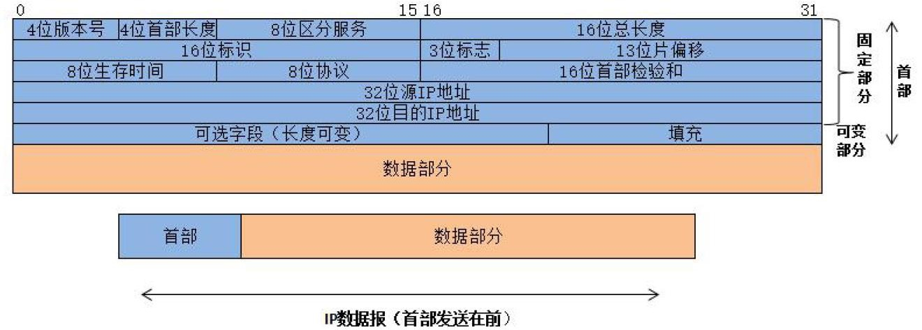
Version: 4 bits, indicating the version of the IP protocol. The current IP protocol version number is 4 (i.e., IPv4);
Header length: 4 bits. The maximum value that can be represented is 15 units (one unit is 4 bytes), so the maximum IP header length is 60 bytes;
Differentiated services: 8 bits, used to obtain better service. In the old standard, it was called the type of service, but in fact it has never been used. In 1998, this field was renamed differentiated services. Only when differentiated services (DiffServ) are used does this field take effect. Generally, this field is not used;
Total length: 16 bits, indicating the total length of the header and data, in bytes, so the maximum length of a datagram is 65535 bytes. The total length must not exceed the maximum transmission unit MTU;
Identification: 16 bits. It is a counter used to generate datagram identification;
Flag: 3 bits. Currently only the first two bits are meaningful.
The lowest bit of the flag field is MF (More Fragment). MF=1 means there are "more fragments" behind. MF=0 means the last fragment.
The middle bit of the flag field is DF (Don't Fragment). Fragmentation is allowed only when DF=0.
Fragment offset: 12 bits, indicating the relative position of a fragment in the original group after a longer group is fragmented. The fragment offset is in units of 8 bytes;
Time to live: 8 bits, denoted as TTL (Time To Live). The maximum number of routers a datagram can pass through in the network. The TTL field is an 8-bit field initially set by the sender. The recommended initial value is specified by the assigned numbers RFC, and the current value is 64. When sending an ICMP echo reply, TTL is often set to the maximum value of 255;
Protocol: 8 bits, indicating which protocol the data carried by this datagram uses, so that the IP layer of the destination host knows which process to deliver the data part to. 1 means ICMP protocol, 2 means IGMP protocol, 6 means TCP protocol, and 17 means UDP protocol;
Header checksum: 16 bits. It only checks the header of the datagram, not the data part. It uses binary one's complement addition, i.e., adds the 16-bit data, then adds the carry to the lower 16 bits until the carry is 0, and finally inverts the 16 bits;
Source address and destination address: each occupies 4 bytes, recording the source address and destination address respectively;
7.2.2.4 UDP Protocol
UDP is the abbreviation of User Datagram Protocol. UDP only provides a basic, low-latency communication called a datagram. A datagram is a data packet with its own addressing information that goes from the sender to the receiver. The UDP protocol is often used in occasions with high requirements for data transmission speed, such as image transmission and network monitoring data exchange.
The header format of the UDP protocol:
The UDP header consists of 4 fields, each occupying 2 bytes, as follows:
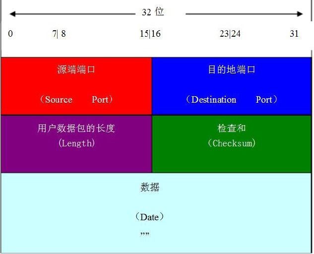
① UDP source port number
② Destination port number
③ Datagram length
④ Checksum
The UDP protocol uses port numbers to retain separate data transmission channels for different applications. The data sender sends the UDP datagram out through the source port, and the data receiver receives the data through the destination port.
The length of the datagram refers to the total number of bytes including the header and data part. Because the header length is fixed, this field is mainly used to calculate the variable-length data part (also called data payload). The maximum length of a datagram varies depending on the operating environment. Theoretically, the maximum length of a datagram including the header is 65535 bytes. However, some practical applications often limit the datagram size, sometimes down to 8192 bytes.
The UDP protocol uses the checksum in the header to ensure data security. The checksum is first calculated by the sender through a special algorithm, and after being passed to the receiver, it needs to be recalculated. If a datagram is tampered with by a third party during transmission or damaged due to line noise, the checksum calculations of the sender and receiver will not match, so the UDP protocol can detect errors. Although UDP provides error detection, when an error is detected, there is no error correction — it just discards the damaged message segment or provides warning information to the application.
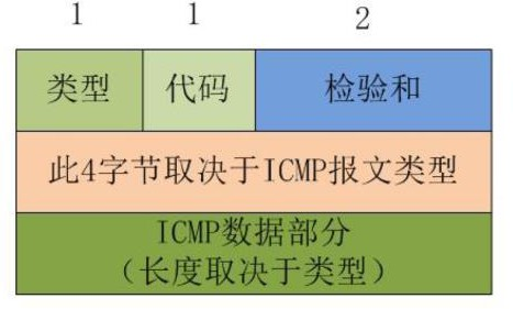
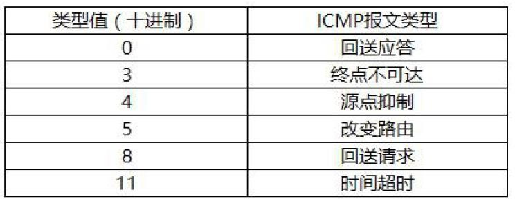
7.2.2.5 Ping Function
The UDP protocol uses the checksum in the header to ensure data security. The checksum is first calculated by the sender through a special algorithm, and after being passed to the receiver, it needs to be recalculated. If a datagram is tampered with by a third party during transmission or damaged due to line noise, the checksum calculations of the sender and receiver will not match, so the UDP protocol can detect errors. Although UDP provides error detection, when an error is detected, there is no error correction — it just discards the damaged message segment or provides warning information to the application.
7.3 SMI (MDC/MDIO) Bus Interface
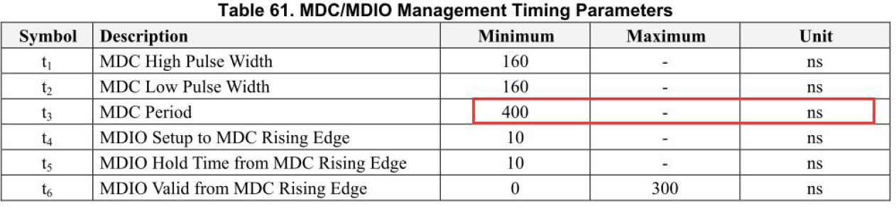
Serial Management Interface, also known as MII Management Interface, includes two signal lines: MDC and MDIO. MDIO is a management interface of the PHY, used to read/write the PHY's registers to control the PHY's behavior or obtain the PHY's status. MDC provides the clock for MDIO and is provided by the MAC end. In this experiment, it is the FPGA end. In the RTL8211EG document, you can see that the minimum period of MDC is 400ns, i.e., the maximum clock is 2.5MHz.
7.3.1 SMI Frame Format
As shown below, the read/write frame format of SMI:

| Name | Description |
|---|---|
| Preamble | Sent by the MAC, 32 consecutive logic "1"s, synchronized with the MDC signal, used for synchronization between MAC and PHY; |
| ST | Frame start bit, fixed at 01 |
| OP | Operation code, 10 means read, 01 means write |
| PHYAD | PHY address, 5 bits |
| REGAD | Register address, 5 bits |
| TA | Turn Around, MDIO direction conversion. In the write state, no direction conversion is needed, value is 10. In the read state, the MAC output is in high-impedance state, and in the second cycle, the PHY pulls MDIO low |
| DATA | 16 bits of data |
| IDLE | Idle state; in this state, MDIO is in high-impedance state, pulled high by an external pull-up resistor |
7.3.2 Read Timing
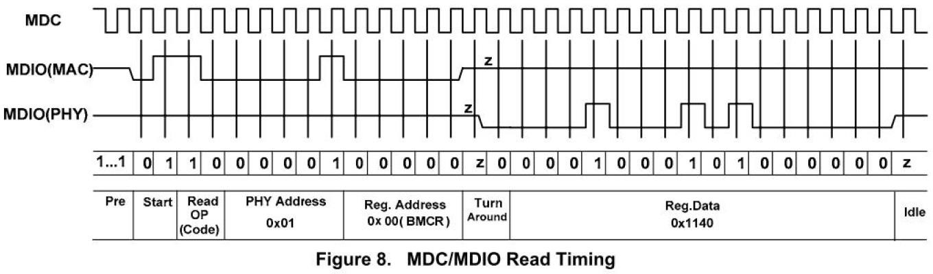
You can see that in the Turn Around state, in the first cycle, MDIO is in high-impedance state, and in the second cycle, it is pulled low by the PHY end.
7.3.3 Write Timing
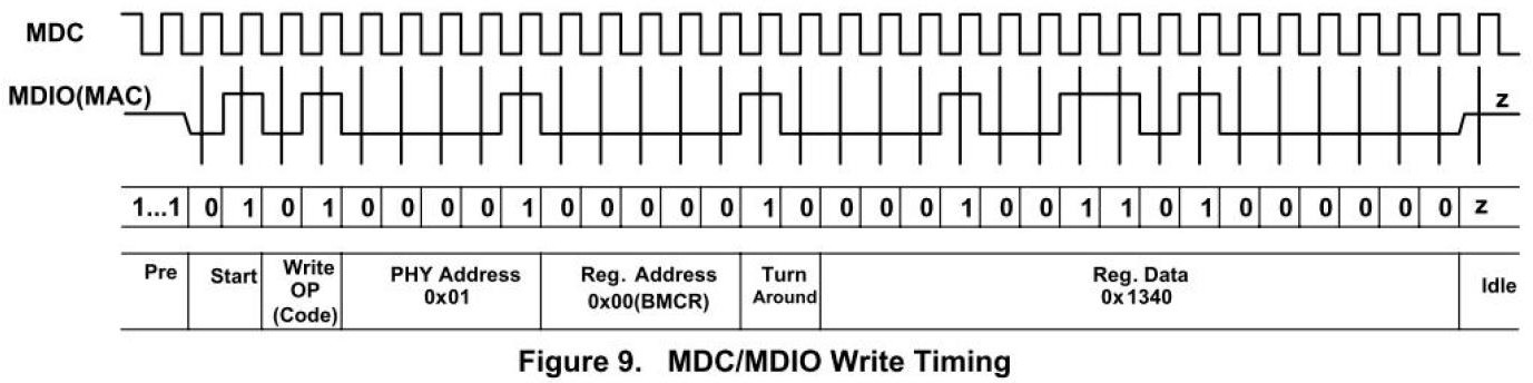
To ensure that data can be correctly sampled, the data is prepared before the rising edge of MDC. In this experiment, data is sent on the falling edge and received on the rising edge.
7.4 Experiment Design
This experiment takes gigabit Ethernet RGMII communication as an example to design the verilog program. It first sends preset UDP data to the network, sending once per second. The program is divided into two parts: sending and receiving, implementing ARP and UDP functions.
7.4.1 Sending Part
7.4.1.1 MAC Layer Sending
In the sending part, mac_tx.v is the MAC layer sending module. First, in the SEND_START state, it waits for the mac_tx_ready signal. If valid, it means the IP or ARP data is ready and sending can begin. Then it enters the send preamble state. When finished, it sends mac_data_req to request IP or ARP data, then enters the send data state, and finally enters the send CRC state. During data sending, CRC check must be performed simultaneously. After the preamble is completed, the upper-layer protocol data is sent out. At the same time, this upper-layer data is put into the CRC32 module for sequence generation. The upper-layer protocol gives a data output completion flag signal. At this time, mac_tx knows that the data sending is complete and needs to end the CRC32 sequence generation. At this point, the FCS is extracted, and after the data is connected, it is sent out. In this way, the preamble — data (MAC frame) — FCS are connected. Then it jumps to the end state, and then returns to the IDLE state, waiting for the next send request.
| Signal Name | Direction | Width | Description |
|---|---|---|---|
| clk | input | 1 | System clock |
| rstn | input | 1 | Active-low reset |
| mac_frame_data | input | 8 | Data from IP or ARP |
| mac_tx_req | input | 1 | MAC send request |
| mac_tx_ready | input | 1 | IP or ARP data is ready |
| mac_tx_end | input | 1 | IP or ARP data transmission is complete |
| mac_tx_data | output | 8 | Data sent to PHY |
| mac_send_end | output | 1 | MAC data send complete |
| mac_data_valid | output | 1 | MAC data valid signal, i.e., gmii_tx_en |
| mac_data_req | output | 1 | MAC layer requests data from IP or ARP |
| mac_tx_ack | output | 1 | MAC layer send data acknowledgement for UPPER request |
7.4.1.2 MAC Send Mode
The mac_tx_mode.v in the project is the send mode selection. It selects the corresponding signals and data based on whether the send mode is IP or ARP.
| Signal Name | Direction | Width | Description |
|---|---|---|---|
| clk | input | 1 | System clock |
| rstn | input | 1 | Active-low reset |
| mac_send_end | input | 1 | MAC send complete |
| arp_tx_req | input | 1 | ARP send request |
| arp_tx_ready | input | 1 | ARP data is ready |
| arp_tx_data | input | 8 | ARP data |
| arp_tx_end | input | 1 | ARP data sending to MAC layer complete |
| arp_tx_ack | input | 1 | ARP send response signal |
| ip_tx_req | input | 1 | IP send request |
| ip_tx_ready | input | 1 | IP data is ready |
| ip_tx_data | input | 8 | IP data |
| ip_tx_end | input | 1 | IP data sending to MAC layer complete |
| mac_tx_ready | output | 1 | MAC data is ready signal |
| ip_tx_ack | output | 1 | IP send response signal |
| mac_tx_ack | output | 1 | MAC send response signal |
| mac_tx_req | output | 1 | MAC send request |
| mac_tx_data | output | 8 | MAC send data |
| mac_tx_end | output | 1 | MAC data send complete |
7.4.1.3 ARP Sending
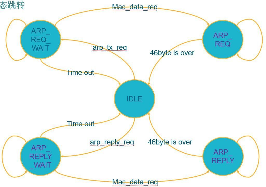
In the sending part, arp_tx.v is the ARP sending module. In the IDLE state, it waits for the ARP send request or ARP reply request signal, then enters the request or reply wait state, and notifies the MAC layer that the data is ready. After waiting for the mac_data_req signal, it enters the request or reply data send state. Since the data is less than 46 bytes, it needs to be padded to 46 bytes for sending.
| Signal Name | Direction | Width | Description |
|---|---|---|---|
| clk | input | 1 | System clock |
| rstn | input | 1 | Active-low reset |
| dest_mac_addr | input | 48 | Destination MAC address to send |
| sour_mac_addr | input | 48 | Source MAC address to send |
| sour_ip_addr | input | 32 | Source IP address to send |
| dest_ip_addr | input | 32 | Destination IP address to send |
| mac_data_req | input | 1 | MAC layer data request signal |
| arp_request_req | input | 1 | ARP request signal |
| arp_reply_ack | output | 1 | ARP reply acknowledgement signal |
| arp_reply_req | input | 1 | ARP reply request signal |
| arp_rec_sour_ip_addr | input | 32 | Source IP address received by ARP, put into destination IP address when replying |
| arp_rec_sour_mac_addr | input | 48 | Source MAC address received by ARP, put into destination MAC address when replying |
| mac_send_end | input | 1 | MAC send complete |
| mac_tx_ack | input | 1 | MAC send acknowledgement |
| arp_tx_ready | output | 1 | ARP data ready |
| arp_tx_data | output | 8 | ARP send data |
| arp_tx_end | output | 1 | ARP data send complete |
| arp_tx_req | output | 1 | ARP send request signal |
7.4.1.4 IP Layer Sending
In the sending part, ip_tx.v is the IP layer sending module. In the IDLE state, if ip_tx_req is valid, i.e., UDP or ICMP send request signal, it enters the wait-for-send-data-length state, then enters the generate-checksum state. The checksum sums all data in the IP header in 16-bit units, then adds the carry to the lower 16 bits until the carry is 0, then inverts the lower 16 bits to obtain the checksum result.
After generating the checksum, it waits for the MAC layer data request, starts sending data, and requests UDP or ICMP data after sending the IP header. After sending, it enters the IDLE state.
| Signal Name | Direction | Width | Description |
|---|---|---|---|
| clk | input | 1 | System clock |
| rstn | input | 1 | Active-low reset |
| dest_mac_addr | input | 48 | Destination MAC address to send |
| sour_mac_addr | input | 48 | Source MAC address to send |
| sour_ip_addr | input | 32 | Source IP address to send |
| dest_ip_addr | input | 32 | Destination IP address to send |
| ttl | input | 8 | Time to live |
| ip_send_type | input | 8 | Upper-layer protocol number, e.g., UDP, ICMP |
| upper_layer_data | output | 8 | Data from UDP or ICMP |
| upper_data_req | input | 1 | Request data from upper layer |
| mac_tx_ack | input | 1 | MAC send acknowledgement |
| mac_send_end | input | 1 | MAC send complete signal |
| mac_data_req | input | 1 | MAC layer data request signal |
| upper_tx_ready | input | 1 | Upper-layer UDP or ICMP data is ready |
| ip_tx_req | input | 1 | Send request, from upper layer |
| ip_send_data_length | input | 16 | Total length of data sent |
| ip_tx_ack | output | Generate IP send acknowledgement | |
| ip_tx_ready | output | 1 | IP data is ready |
| ip_tx_data | output | 8 | IP data |
| ip_tx_end | output | 1 | IP data sending to MAC layer complete |
7.4.1.5 IP Send Mode
The ip_tx_mode.v in the project is the send mode selection. It selects the corresponding signals and data based on whether the send mode is UDP or ICMP.
| Signal Name | Direction | Width | Description |
|---|---|---|---|
| clk | input | 1 | System clock |
| rstn | input | 1 | Active-low reset |
| mac_send_end | input | MAC data send complete | |
| udp_tx_req | input | 1 | UDP send request |
| udp_tx_ready | input | 1 | UDP data ready |
| udp_tx_data | input | 8 | UDP send data |
| udp_send_data_length | input | 16 | UDP send data length |
| udp_tx_ack | output | 1 | Output UDP send acknowledgement |
| icmp_tx_req | input | 1 | ICMP send request |
| icmp_tx_ready | input | 1 | ICMP data ready |
| icmp_tx_data | input | 8 | ICMP send data |
| icmp_send_data_length | input | 16 | ICMP send data length |
| icmp_tx_ack | output | 1 | ICMP send acknowledgement |
| ip_tx_ack | input | 1 | IP send acknowledgement |
| ip_tx_req | input | 1 | IP send request |
| ip_tx_ready | output | 1 | IP data is ready |
| ip_tx_data | output | 8 | IP data |
| ip_send_type | output | 8 | Upper-layer protocol number, e.g., UDP, ICMP |
| ip_send_data_length | output | 16 | Total length of data sent |
7.4.1.6 UDP Sending
In the sending part, udp_tx.v is the UDP sending module.
| Signal Name | Direction | Width | Description |
|---|---|---|---|
| clk | input | 1 | System clock |
| rstn | input | 1 | Active-low reset |
| app_data_in_valid | input | 1 | Data output valid signal received from external |
| app_data_in | input | 8 | Data received from external |
| app_data_length | input | 16 | Length of the current data packet received from external (excluding udp, ip, mac headers) |
| udp_dest_port | input | 16 | Source port number of the data packet received from external |
| app_data_request | input | 1 | User interface data send request |
| udp_send_ready | output | 1 | UDP data send preparation |
| udp_send_ack | output | 1 | UDP data send acknowledgement |
| ip_send_ready | input | 1 | IP data send preparation |
| ip_send_ack | input | 1 | IP data send acknowledgement |
| udp_send_request | output | 1 | User interface data send request |
| udp_data_out_valid | output | 1 | Send data output valid signal |
| udp_data_out | output | 8 | Send data output |
| udp_packet_length | output | 16 | Length of the current data packet (excluding udp, ip, mac headers) |
7.4.2 Receiving Part
7.4.2.1 MAC Layer Receiving
In the receiving part, mac_rx.v is the MAC layer receiving file. First, in the IDLE state, when rx_en is high, it enters the REC_PREAMBLE preamble state to receive the preamble. Then it enters the receive MAC header state, i.e., destination MAC address, source MAC address, type. They are cached, and in this state, it determines whether the preamble is correct. If wrong, it enters the REC_ERROR error state. In the REC_IDENTIFY state, it determines whether the type is IP (8'h0800) or ARP (8'h0806). Then it enters the receive data state, transfers the data to the IP or ARP module, waits for the IP or ARP data reception to complete, and then receives the CRC data. During the data reception process, CRC processing is performed on the received data, and the result is compared with the received CRC data to determine whether the data is received correctly. If correct, it ends; if wrong, it enters the ERROR state.
| Signal Name | Direction | Width | Description |
|---|---|---|---|
| clk | input | 1 | System clock |
| rstn | input | 1 | Active-low reset |
| rx_en | input | 1 | Start receive enable |
| mac_rx_datain | input | 8 | Received data |
| checksum_err | input | 1 | IP layer checksum error signal |
| ip_rx_end | input | 1 | IP receive complete |
| arp_rx_end | input | 1 | ARP receive complete |
| ip_rx_req | output | 1 | IP receive request |
| arp_rx_req | input | 1 | Request ARP receive |
| mac_rx_dataout | output | 8 | MAC layer receive data output to IP or ARP |
| mac_rec_error | output | 1 | MAC layer receive error |
| mac_rx_dest_mac_addr | output | 48 | Destination IP address received by MAC |
| mac_rx_sour_mac_addr | output | 48 | Source IP address received by MAC |
7.4.2.2 ARP Receiving
The arp_rx.v in the project is the ARP receiving module, which implements ARP data reception. In the IDLE state, after receiving the arp_rx_req signal sent from the MAC layer, it enters the ARP receive state. In this state, it extracts the destination MAC address, source MAC address, destination IP address, and source IP address, and determines whether the operation code OP is a request or a reply. If it is a request, it determines whether the received destination IP address is the local address. If yes, it sends the reply request signal arp_reply_req. If not, it is ignored. If OP is a reply, it determines whether the received destination IP address and destination MAC address are consistent with the local machine. If yes, it pulls the arp_found signal high, indicating that the other party's address has been received. The other party's MAC address and IP address are stored in the ARP cache.
| Signal Name | Direction | Width | Description |
|---|---|---|---|
| clk | input | 1 | System clock |
| rstn | input | 1 | Active-low reset |
| local_ip_addr | input | 32 | Local IP address |
| local_mac_addr | input | 48 | Local MAC address |
| arp_rx_data | input | 8 | ARP receive data |
| arp_rx_req | input | 1 | ARP receive request |
| arp_rx_end | output | 1 | ARP receive complete |
| arp_reply_ack | input | 1 | ARP reply acknowledgement |
| arp_reply_req | output | 1 | ARP reply request |
| arp_rec_sour_ip_addr | input | 32 | Source IP address received by ARP |
| arp_rec_sour_mac_addr | input | 48 | Source MAC address received by ARP |
| arp_found | output | 1 | ARP received request/reply correct |
7.4.2.3 IP Layer Receiving Module
In the project, ip_rx is the IP layer receiving module, which implements IP layer data reception, information extraction, and checksum check. First, in the IDLE state, it judges the ip_rx_req signal sent from the MAC layer, and enters the receive IP header state. First, in REC_HEADER0, it extracts the header length and IP total length, and enters the REC_HEADER1 state. In this state, it extracts the destination IP address, source IP address, and protocol type, and sends udp_rx_req or icmp_rx_req according to the protocol type. While receiving the header, it performs a checksum check, summing all the data received in the header, storing it in a 32-bit register, then adding the high 16 bits
to the low 16 bits until the high 16 bits are 0, then inverting the low 16 bits, and determining whether it is 0. If 0, the check is correct; otherwise, it is wrong. It enters the IDLE state, discards this frame of data, and waits for the next reception.
| Signal Name | Direction | Width | Description |
|---|---|---|---|
| clk | input | 1 | System clock |
| rstn | input | 1 | Active-low reset |
| local_ip_addr | input | 32 | Local IP address |
| local_mac_addr | input | 48 | Local MAC address |
| ip_rx_data | input | 8 | Data received from MAC layer |
| ip_rx_req | input | 1 | IP receive request signal sent by MAC layer |
| mac_rx_dest_mac_addr | input | 48 | Destination MAC address received by MAC layer |
| udp_rx_req | output | 1 | UDP receive request signal |
| icmp_rx_req | output | 1 | ICMP receive request signal |
| ip_addr_check_error | output | 1 | Address check error signal |
| upper_layer_data_length | output | 16 | Upper-layer protocol data length |
| ip_total_data_length | output | 16 | Total data length |
| net_protocol | output | 8 | Network protocol number |
| ip_rec_source_addr | output | 32 | Source IP address received by IP layer |
| ip_rec_dest_addr | output | 32 | Destination IP address received by IP layer |
| ip_rx_end | output | 1 | IP layer receive complete |
| ip_checksum_error | output | 1 | IP layer checksum check error signal |
7.4.2.4 UDP Receiving
In the project, udp_rx.v is the UDP receiving module. In this module, the UDP header is received first, then the data part is received. While receiving, UDP checksum check is performed. If the UDP data has an odd number of bytes, 8'h00 is appended after the last byte for checksum calculation. The check method is the same as the IP checksum. If the check is correct, the udp_rec_data_valid signal is pulled high, indicating that the received UDP data is valid; otherwise, it is invalid, waiting for the next reception.
| Signal Name | Direction | Width | Description |
|---|---|---|---|
| clk | input | 1 | System clock |
| rstn | input | 1 | Active-low reset |
| udp_rx_data | input | 8 | UDP receive data |
| udp_rx_req | input | 1 | UDP receive request |
| ip_checksum_error | input | 1 | IP layer checksum check error signal |
| ip_addr_check_error | input | 1 | Address check error signal |
| udp_rec_rdata | output | 8 | UDP receive read data |
| udp_rec_data_length | output | 16 | UDP receive data length |
| udp_rec_data_valid | output | 1 | UDP receive data valid |
7.4.3 Other Parts
7.4.3.1 ICMP Reply
In the project, icmp_reply.v implements the ping function. First, it receives the icmp data sent from other devices, determines whether the type is an ECHO REQUEST. If yes, it stores the data in the RAM, calculates the checksum, and determines whether the checksum is correct. If correct, it enters the send state and sends the data out.
| Signal Name | Direction | Width | Description |
|---|---|---|---|
| clk | input | 1 | System clock |
| rstn | input | 1 | Active-low reset |
| mac_send_end | input | 1 | MAC send complete signal |
| ip_tx_ack | input | 1 | IP send acknowledgement |
| icmp_rx_data | input | 8 | ICMP receive data |
| icmp_rx_req | input | 1 | ICMP receive request |
| icmp_rev_error | input | 1 | Receive error signal |
| upper_layer_data_length | input | 16 | Upper-layer protocol length |
| icmp_data_req | input | 1 | Request ICMP data |
| icmp_tx_ready | output | 1 | ICMP send ready |
| icmp_tx_data | output | 8 | ICMP send data |
| icmp_tx_end | output | 1 | ICMP send complete |
| icmp_tx_req | output | 1 | ICMP send request |
7.4.3.2 ARP Cache
In the project, arp_cache.v is the arp cache module. It caches the IP addresses and MAC addresses of other devices received. Before sending data, it queries whether the destination address exists. If not, it sends an ARP request to the destination address and waits for a reply. In the design file, only one cache space is made. If needed, it can be extended.
| Signal Name | Direction | Width | Description |
|---|---|---|---|
| clk | input | 1 | System clock |
| rstn | input | 1 | Active-low reset |
| arp_found | input | 1 | ARP reply received correctly |
| arp_rec_source_ip_addr | input | 32 | Source IP address received by ARP |
| arp_rec_source_mac_addr | input | 48 | Source MAC address received by ARP |
| dest_ip_addr | input | 32 | Destination IP address |
| dest_mac_addr | output | 48 | Destination MAC address |
| mac_not_exist | output | 1 | The MAC address corresponding to the destination address does not exist |
7.4.3.3 CRC Check Module (crc.v)
The CRC32 check is calculated starting from the destination MAC address and continues until the last data of a packet. Some websites can automatically generate verilog files for the CRC algorithm: https://bues.ch/cms/hacking/crcgen.html
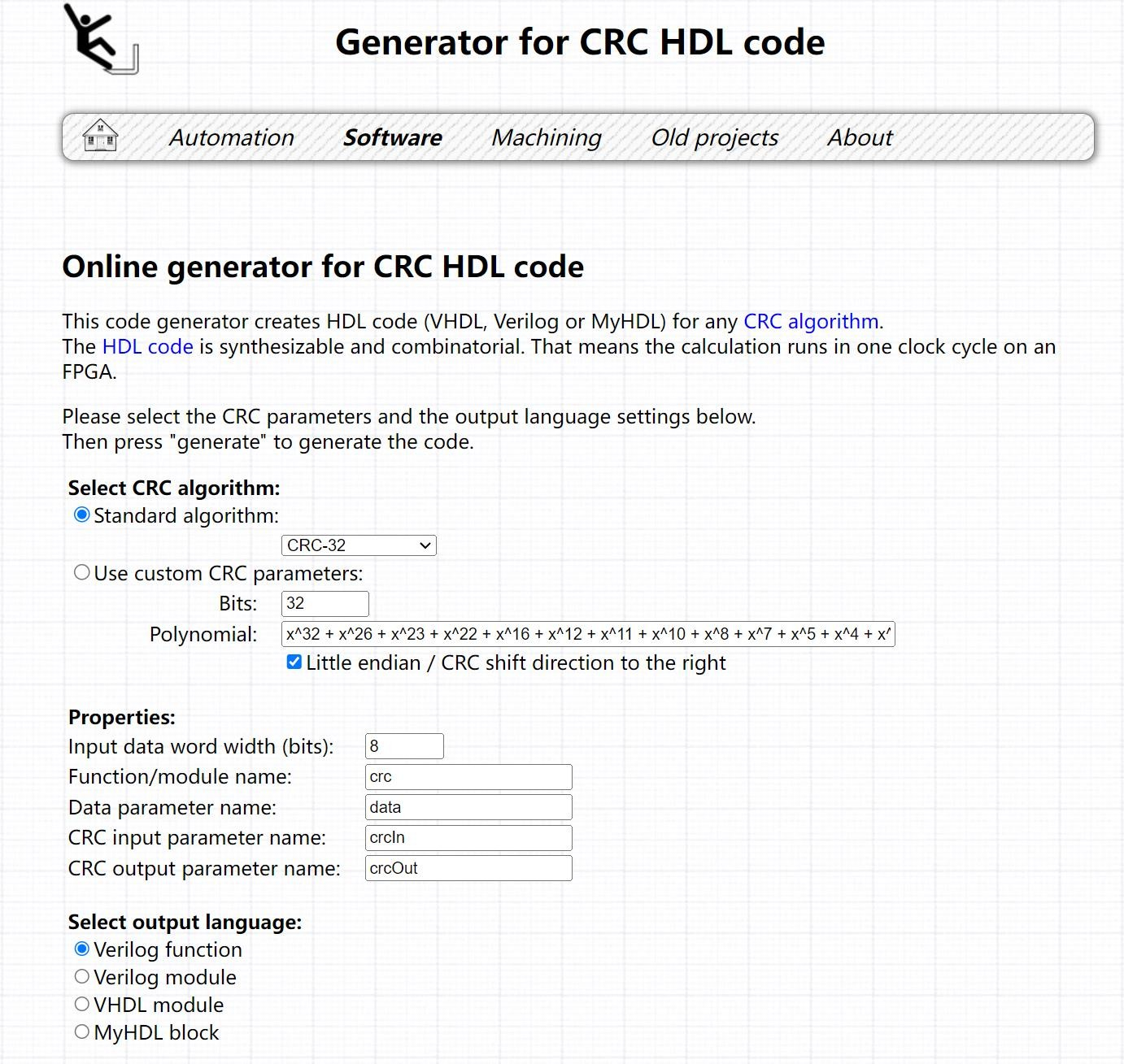
7.5 Experiment Phenomenon
Plug the photoelectric conversion module into the SFP port, and then connect it to the PC network port with a network cable;
Set the receiver (PC) IP address to 192.168.0.3, and the development board IP address to 192.168.0.2, as shown below:

Through the command prompt, enter arp -a. You can find IP: 192.168.0.2, MAC: a0_b1_c2_d3_e1_e1;
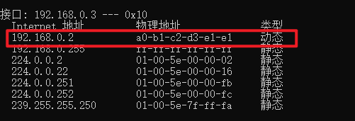
Use Wireshark software to capture packets to verify whether the data link is connected normally and whether data transmission is normal. In the package, open Wireshark software on the PC side. After burning again, capture the datagram and you can see the interaction process shown below.
After the connection is successfully established, the datagram "www.meyesemi.com" will be continuously sent. As shown below:
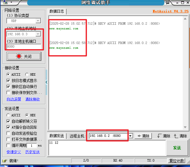
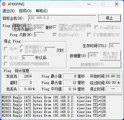
Ping function test. As can be seen from the figure above, ping basically has no packet loss.
8 PCIe-Based DMA/PIO Control Experiment
8.1 Function and Performance
PCIe DMA implements the business function of memory read/write requests and converts the AXI4-Stream interface into a RAM read/write interface for user convenience. Users can read and write the RAM inside the FPGA via PIO and DMA on the CPU side;
The DMA application scenario is shown in Figure 1;
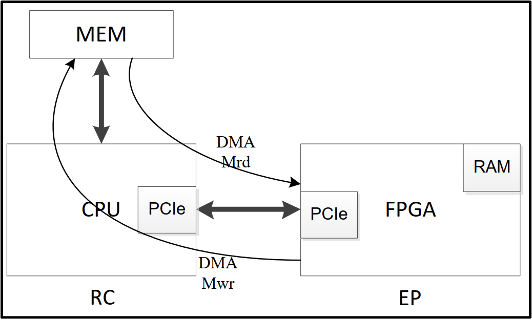
The main functions supported by the PCIe DMA routine are as follows;
- Supports Gen1x1, Gen1x2, Gen1x4, Gen2x1, Gen2x2, Gen2x4;
- Supports memory read operation (Mrd);
- Supports memory write operation (Mwr);
- Supports Max Payload Size of 128Byte, 256Byte, 512Byte, 1024Byte data transmission;
- Converts AXI4-Stream interface into a RAM read/write interface.
8.2 Principle and Implementation
8.2.1 RTL Implementation of DMA
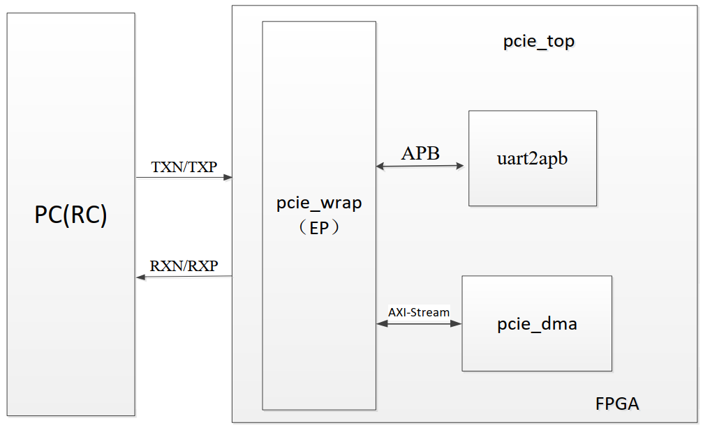
PCIe DMA mainly includes uart2apb and pcie_dma. The main function of uart2apb is to introduce external control to configure the working mode of PCIe. By default, it is in EP mode controlled by RC for DMA and PIO. The main function of the pcie_dma module is to receive TLP packet data output by the PCIe hard IP, and to compose the data to be sent to the RC into TLP packets and send them to the PCIe hard IP. Internally, the data written to the FPGA by PIO and DMA is stored in different BRAMs.
8.2.2 PCIe DMA Module
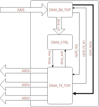
The DMA operation flow is shown below:
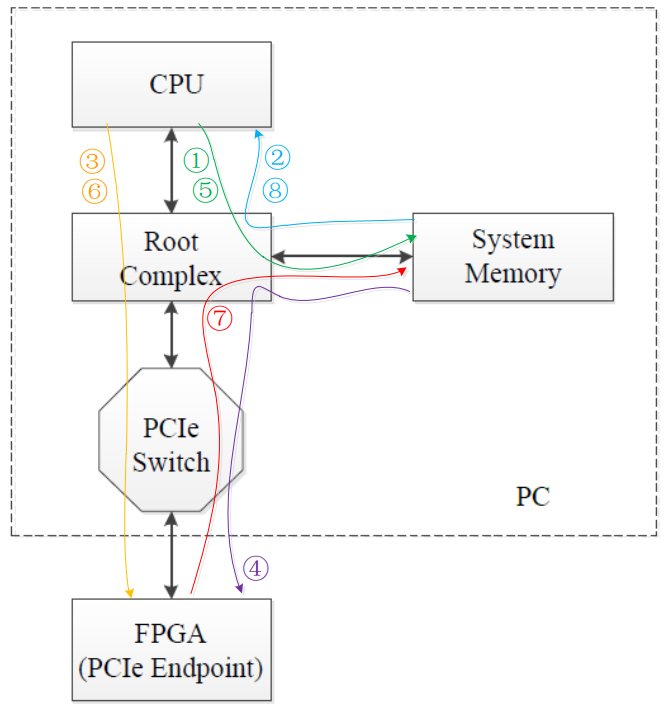
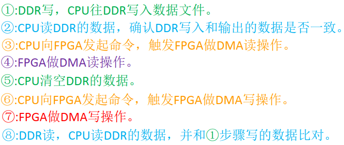
The AXI4-Stream Master interface timing for PCIe data interaction is shown below; the first Cycle of axis_master_tdata is the TLP Header, and axis_master_tkeep is all 1s in the TLP Header field;
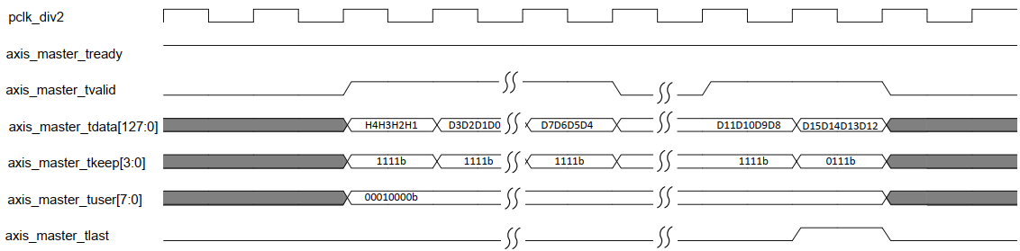
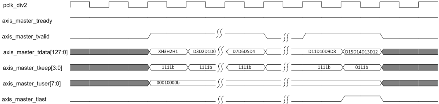
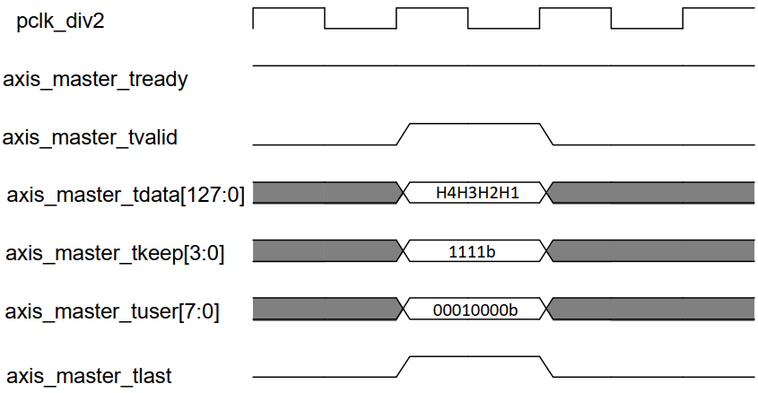
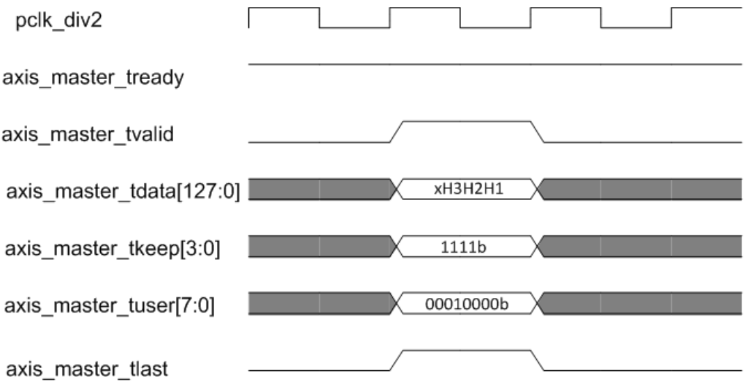
The AXI4-Stream slave interface timing for PCIe data interaction is shown above; once the axis_slave bus starts sending data, axis_slave0/1/2_tvalid must remain high until the last data is transmitted (axis_slave0/1/2_tlast high pulse) before it can be pulled low.
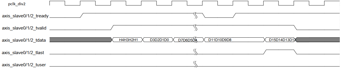
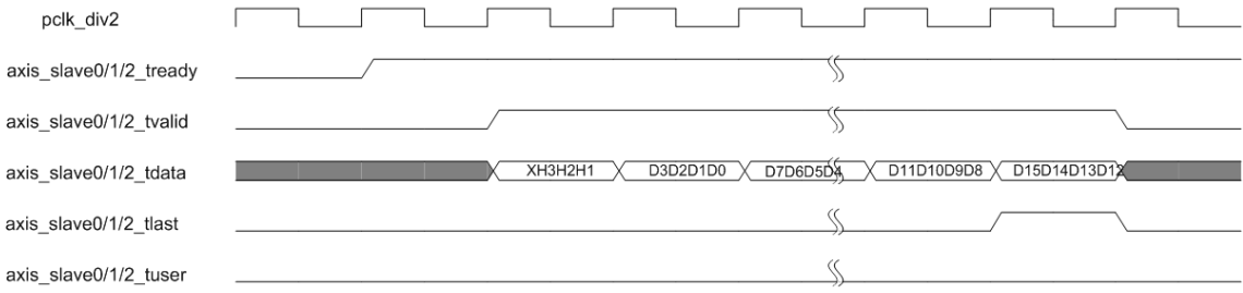
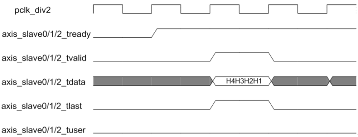
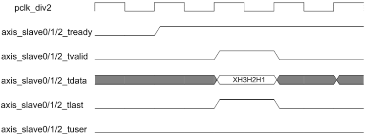
8.2.2.1 dma_rx_top Module
The main function of this module is to parse TLP packets from PCIe and save the data written by RC to EP (PIO/DMA) into BRAM for later use;
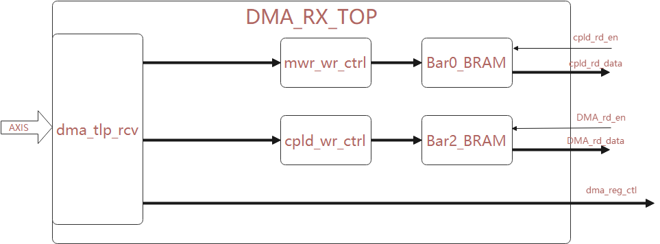
- dma_tlp_rcv module
The main function of this module is to receive and parse TLP protocol packets from the AXIS_Master interface, output the parsed payload data, and the identification information of the data channel to the following mwr_wr_ctrl, cpld_wr_ctrl, and dma_ctrl modules; completing the first functional link of interaction with PCIe;
- mwr_wr_ctrl module
The main function of this module is to pre-process the parsed mwr-type (mwr, IOwr) packet data, output the signals corresponding to the BRAM write interface, and then write them into Bar0_BRAM; for that RC system, this module is the conversion module for PIO writes;
- cpld_wr_ctrl module
After receiving the Mrd packet sent by EP, the DMA bus on the RC side reads data from the storage and forms a Cpld packet to send down to the EP side. The main function of this module is to pre-process the parsed Cpld packet data, output the signals corresponding to the BRAM write interface, and then write them into Bar1_BRAM; for that RC system, this module is the conversion module for DMA_RD writes;
- BRAM module
Both BRAM modules call the Block RAM in the FPGA. During the test, RC must first perform a write operation on the RAM, and then the read-up can correspond one-to-one;
8.2.2.2 dma_tx_top Module
The function of this module is to send the data in the FPGA to the PCIe interface. There are 3 AXIS interfaces in total; in this test program, each of the 3 axis sends a different type of packet; AXIS_slave0 connects to the Cpld packet fed back by the FPGA, acknowledging the Mrd/IOrd packet issued by RC; AXIS_slave1 connects to the Mrd packet actively initiated by the FPGA. The FPGA fetches RC's DDR data; AXIS_slave2 connects to the Mwr packet actively initiated by the FPGA. The FPGA writes data to RC's DDR;
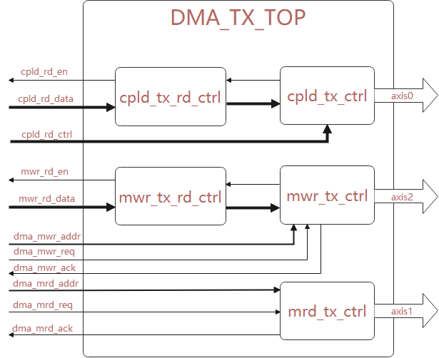
- cpld_tx_ctrl module
This module is triggered by the Cpld-related control signal parsed by the RX_TOP module and starts to compose the Cpld packet. It initiates a data fetch request to the cpld_tx_rd_ctrl module, and after receiving the data, composes a Cpld Tlp packet and outputs it to the PCIe hard core;
- cpld_tx_rd_ctrl module
After receiving the data fetch request initiated by the cpld_tx_ctrl module, this module converts it into a BRAM read interface signal, initiates a read request to the dma_rx_top module, and after receiving the data, transfers it to the cpld_tx_ctrl module;
- mwr_tx_ctrl module
This module receives the DMA_CTRL module's mwr request, data length, and RC's corresponding address, and starts to prepare to send the Mwr packet. It initiates a data fetch request to the mwr_tx_rd_ctrl module, and after receiving the data, composes an mwr Tlp packet and outputs it to the PCIe hard core;
- mwr_tx_rd_ctrl module
After receiving the data fetch request initiated by the mwr_tx_ctrl module, this module converts it into a BRAM read interface signal, initiates a read request to the dma_rx_top module, and after receiving the data, transfers it to the mwr_tx_ctrl module;
- mrd_tx_ctrl module
This module receives the DMA_CTRL module's mrd request, data length, and RC's corresponding address, and starts to prepare to send the Mrd packet. It composes an mwr Tlp packet and outputs it to the PCIe hard core;
8.2.2.3 dma_ctrl Module
The RC side sends down the relevant control signals through Bar1's register space to control the FPGA for the corresponding DMA channel control; the corresponding control registers and parsing are as follows;
| Register Address | Function Name | Description | Parsing |
|---|---|---|---|
| Bar1_base_addr + 0x100 | Dma_cmd_reg | DMA command register | [9:0] : DMA transfer length [16] : DMA address length 0: 32bit 1: 64bit [24]:DMA packet type 0: Mrd 1: Mwr |
| Bar1_base_addr + 0x110 | Dma_cmd_l_addr | DMA transfer address low | [ 1:0] : Reserved [31:0] : dma_addr[31:2] |
| Bar1_base_addr + 0x120 | Dma_cmd_h_addr | DMA transfer address high | High 32 bits of MEM access address |
8.3 Project Introduction
- Simulation reference design The simulation block diagram of the reference design is shown in the figure.
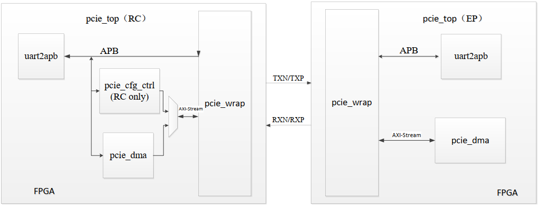
Simulation environment: third-party simulation software. Run script: sim.bat Simulation filelist: pango_pcie_top_filelist.f. The simulation waveform is shown below.
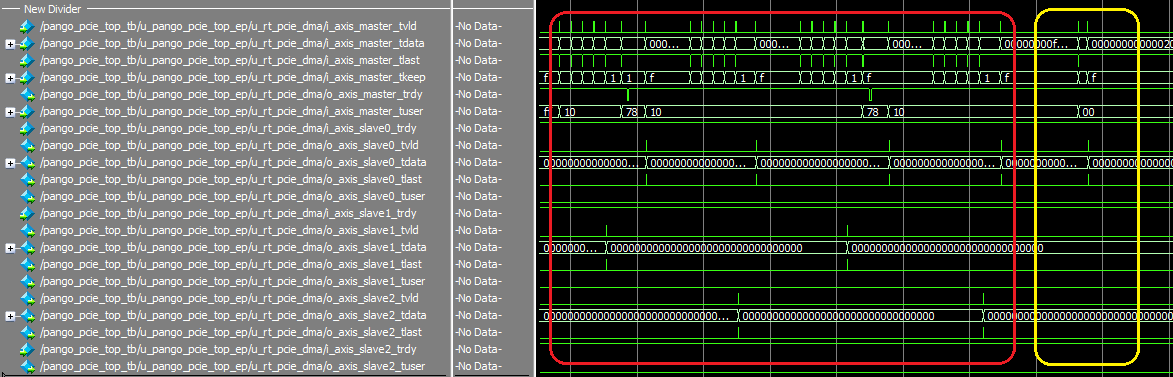
- On-board testing
Before the docking test, ensure the following operations are correct:
- Ensure that the driver is installed successfully.
- Confirm that the FPGA has flashed the firmware into Flash;
- Ensure the design project fdc constraints are correct. The reference design fdc constraint file provides Gen1x1 mode and Gen2x2 mode.